
FOUP wafer carriers are the backbone of modern 300mm semiconductor fabrication. These front‑opening unified pods protect wafers during transport, storage, and processing within the fab. They maintain a controlled internal environment, minimise particle contamination, and enable standardised automation. Hiner‑pack offers a comprehensive range of FOUPs designed to meet the stringent requirements of advanced nodes.
As device geometries shrink, the role of the wafer carrier becomes more critical. FOUPs must provide mechanical protection, chemical compatibility, and electrostatic discharge (ESD) safety. They interface with factory automation systems such as overhead hoists (OHT) and equipment load ports. Selecting the right FOUP directly impacts yield and tool uptime.
What Are FOUP Wafer Carriers? Design and Industry Standards
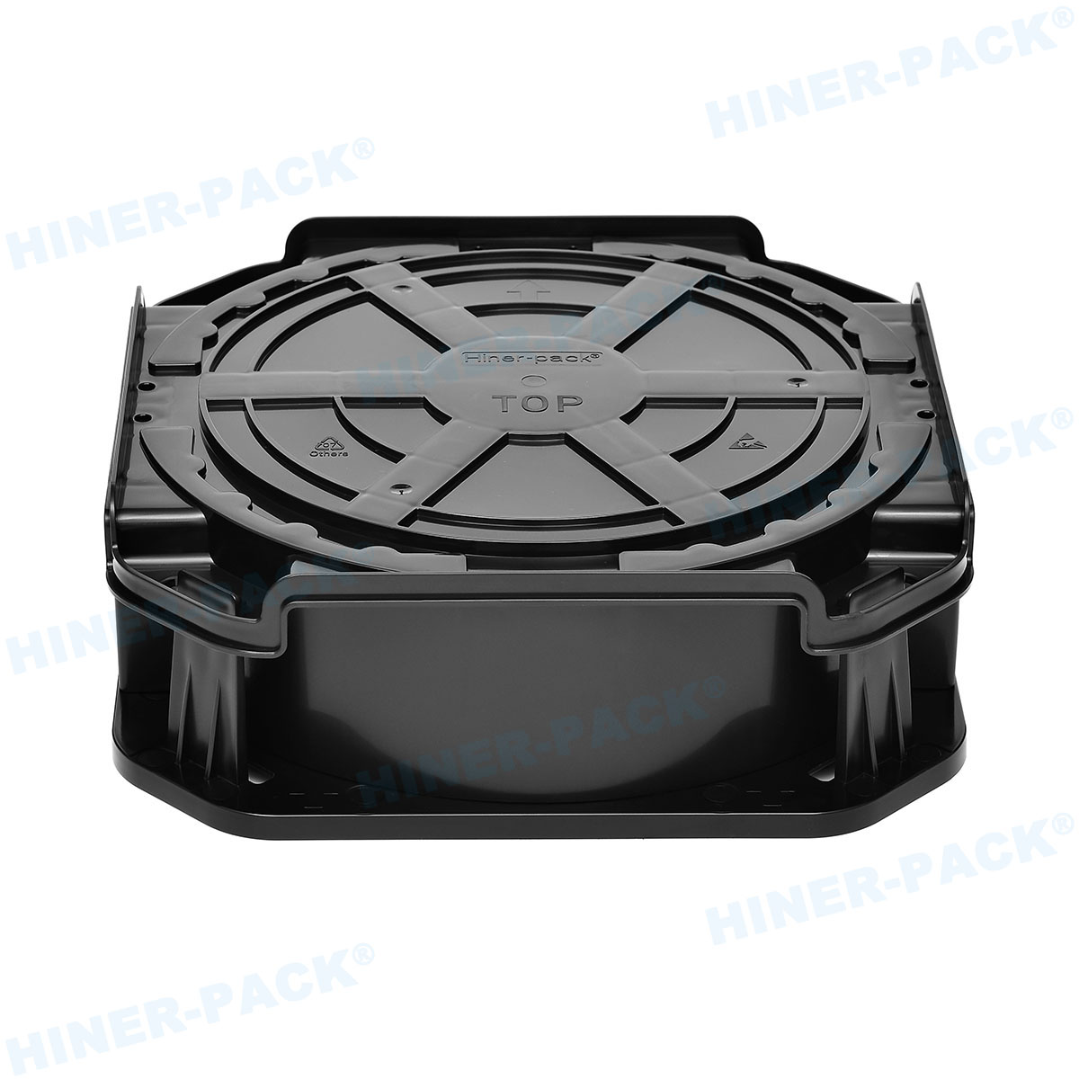
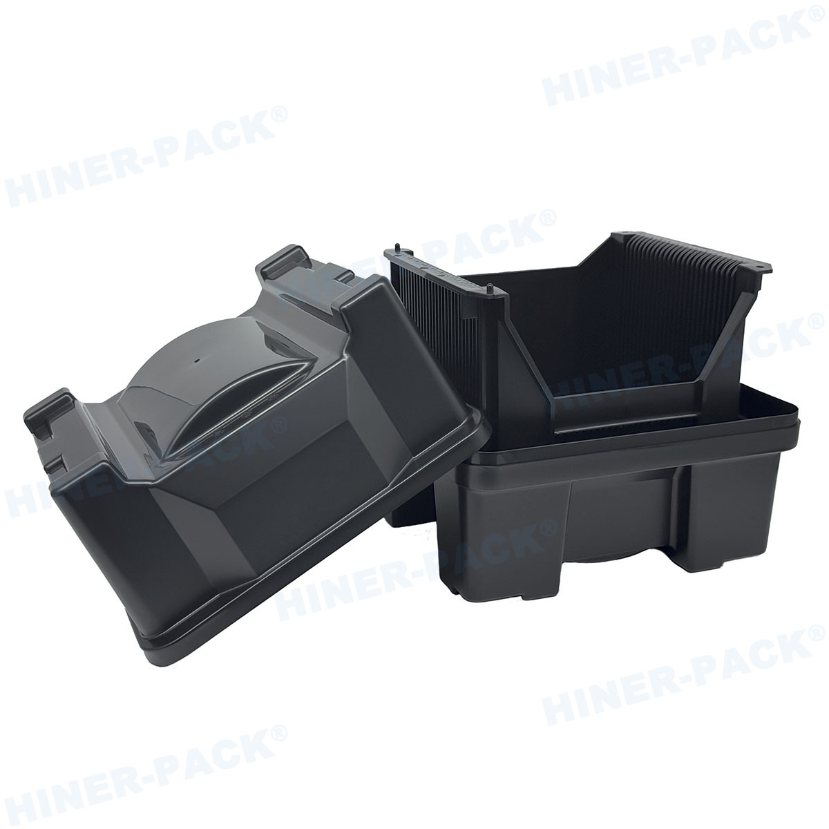
A FOUP wafer carrier is a sealed enclosure with a front door that opens automatically when placed on a load port. It holds up to 25 wafers of 300 mm diameter, supported on specially designed shelves or slots. The interior is continuously purged with nitrogen to prevent native oxide growth and airborne molecular contamination.
SEMI standards: FOUPs conform to SEMI E47.1, E62, and E111, ensuring interoperability across different OEM tools.
Materials: Typically made from polycarbonate blended with carbon powder for conductivity and rigidity.
Integrity: Seals and latches maintain a Class 1 or better internal environment.
Hiner‑pack engineers its FOUPs to exceed these standards, with precision‑moulded components and 100% dimensional inspection.
Key Components of a FOUP
Every FOUP consists of several critical parts: the shell, the door, the wafer supports (pads or combs), a latch mechanism, and an identification tag. The door includes a kinematic coupling plate that aligns the pod to the load port. Wafer supports are often made of a softer polymer to avoid scratching.
Advanced FOUPs incorporate purge ports for nitrogen or clean dry air. Some designs include sensors for humidity, particle count, or tamper detection.
Material and Cleanliness Requirements for FOUP Wafer Carriers
The primary material for FOUPs is polycarbonate (PC) with conductive fillers. This combination provides stiffness, impact resistance, and ESD protection (surface resistivity 10⁵–10⁹ Ω/sq). The carbon loading must be carefully controlled to avoid outgassing or particle shedding.
Particle control: FOUPs are moulded in cleanroom environments and cleaned using CO₂ snow or DI water prior to shipment.
Outgassing: Low‑outgassing polymers are selected to prevent contamination of sensitive gate oxides.
Metal contamination: Trace metals are kept below 10¹⁰ atoms/cm².
Hiner‑pack performs ICP‑MS analysis on every batch of raw material to guarantee purity. Their FOUP wafer carriers are certified for use in 1x nm logic and 3D NAND fabs.
Automation and Interface: FIMS and AMHS Compatibility
FOUPs are designed to work seamlessly with factory automation. The front‑opening interface mechanical standard (FIMS) defines the kinematics, door operation, and mapping flags. When a FOUP is placed on a load port, the port’s door engages with the FOUP door, opens it, and presents the wafers to the robot.
Automated material handling systems (AMHS) transport FOUPs via overhead hoists or rail‑guided vehicles. The pods feature robust top flanges and bottom grooves for secure gripping. Hiner‑pack tests its FOUPs under simulated transport to ensure no wafer slippage or vibration damage.
Selecting the Right FOUP Wafer Carriers for Your Fab
Choice depends on process requirements, wafer size (only 300 mm currently), and specific tool interfaces. Important considerations include:
Purge capability: Some processes require continuous N₂ flow; choose FOUPs with integrated purge ports.
Mapping windows: Optical or capacitive sensors read wafer presence; the FOUP must have clear mapping slots.
ESD performance: For sensitive devices, conductive or dissipative materials are mandatory.
Hiner‑pack offers variants with different slot pitches (10 mm, 12 mm) and custom RFID tag placements. Their engineering team can modify existing designs to match unique fab layouts.
Maintenance and Cleaning of FOUP Wafer Carriers
Regular cleaning prevents cross‑contamination and extends carrier life. Common methods include:
Wet cleaning with deionised water and mild surfactants, followed by vacuum drying.
Dry cleaning using CO₂ pellets or UV‑ozone treatment for organic removal.
Periodic replacement of wear parts such as door seals and wafer cushions.
Fabs typically clean FOUPs every 30–60 days, depending on usage. Hiner‑pack provides a reconditioning service that includes ultrasonic cleaning, surface resistance verification, and particle count testing.
Future Trends: 450 mm FOUPs and Beyond
The industry has explored 450 mm wafer transition, which would require larger FOUPs (approximately 1.5x the size). Material handling and weight become significant challenges. Meanwhile, current innovations focus on smart FOUPs with embedded sensors that monitor environment and log handling history. These smart carriers enable predictive maintenance and process optimisation.
Hiner‑pack participates in consortia developing next‑generation carriers. Their R&D team works on lightweight composites and integrated electronics for future FOUP wafer carriers.
Why Partner with Hiner‑pack for FOUP Wafer Carriers?
Hiner‑pack combines decades of precision plastics experience with deep semiconductor knowledge. Their FOUPs are moulded in ISO Class 4 cleanrooms and tested for dimensional accuracy, particle emission, and ESD performance. They offer rapid prototyping, global logistics, and technical support. By choosing Hiner‑pack, fabs achieve higher equipment uptime and lower defect densities.
In summary, FOUP wafer carriers are an indispensable component of any 300 mm wafer facility. Their design, material purity, and automation compatibility directly influence manufacturing efficiency. With the right partner like Hiner‑pack, semiconductor companies can ensure their wafers are protected from fab start to finish.
Frequently Asked Questions
Q1: What does FOUP stand for, and why is it important?
A1: FOUP stands for Front‑Opening Unified Pod. It is a specialised container that protects 300 mm wafers during transport and storage. Its importance lies in maintaining a clean, controlled micro‑environment and enabling automated handling, which are essential for high‑yield manufacturing.
Q2: How many wafers does a typical FOUP hold?
A2: Standard FOUPs are designed to hold 25 wafers of 300 mm diameter. However, some custom versions accommodate 13 or 6 wafers for engineering runs or small‑lot production.
Q3: What materials are FOUP wafer carriers made of?
A3: Most FOUPs are injection‑moulded from polycarbonate blended with conductive fillers (carbon or carbon nanotubes) to provide ESD protection. The wafer contact points may use PEEK or other low‑particulate polymers.
Q4: How often should FOUPs be cleaned?
A4: Cleaning intervals depend on fab usage and process sensitivity. A common practice is to clean FOUPs every 30 days or after 25–30 runs in critical layers. Fabs with advanced contamination control may extend this to 60 days.
Q5: Can Hiner‑pack provide custom FOUP designs?
A5: Yes, Hiner‑pack specialises in custom‑engineered FOUPs. They work with customers to modify internal slot pitch, add purge features, integrate RFID, or adjust the kinematic coupling to match specific OEM equipment.
Q6: Are FOUPs used for wafer sizes other than 300 mm?
A6: Currently, FOUPs are exclusively used for 300 mm wafers. For 200 mm, the industry uses FOSBs (Front Opening Shipping Boxes) or standard cassettes. 450 mm development also envisions larger FOUP‑like containers.
Q7: How do FOUPs prevent wafer contamination?
A7: FOUPs are sealed with a gasketed door and often purged with nitrogen to displace moisture and oxygen. The conductive materials prevent electrostatic attraction of particles. Regular cleaning and monitoring ensure long‑term cleanliness.


