
In the high-stakes world of semiconductor manufacturing and handling, a single particle of dust or a minor electrostatic discharge (ESD) event can ruin a valuable component. Protecting delicate integrated circuits (ICs), known good die (KGD), multi-chip modules (MCMs), and even full wafers during transport, testing, and storage is not just a logistical step—it's a critical financial and operational imperative. This is where specialized Gel Pak component trays become indispensable. Unlike standard trays or carriers, these solutions employ a unique, non-tacky gel surface to securely hold components without damage, offering unparalleled protection against physical and electrostatic hazards. For companies like Hiner-pack, engineering these trays to meet the exacting demands of the semiconductor industry is a core focus, ensuring that sensitive electronics arrive and are stored in perfect condition.
The Critical Role of Component Protection in Semiconductor Operations
Semiconductor devices become increasingly fragile as geometries shrink and complexity grows. Bare die are especially vulnerable to mechanical damage, such as edge chipping or surface scratches. Furthermore, the industry’s move towards more sophisticated packaging, including fan-out wafer-level packaging (FO-WLP) and 3D integration, demands handling solutions that protect not just the silicon but also delicate interconnect structures.
Traditional vacuum pick-up or mechanical clamping methods pose risks. Gel Pak component trays provide a passive, reliable alternative. The component is gently pressed into the gel, which conforms to its shape and holds it firmly in place via slight suction and even adhesion. This eliminates the need for forceful mechanical clamping that can induce stress or damage.
Core Design Features of Advanced Gel Pak Trays
Hiner-pack engineers its trays around several non-negotiable features required for semiconductor applications.
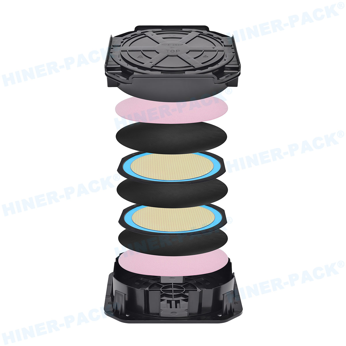
First is the gel formulation itself. It must be cleanroom-compatible, non-outgassing, and chemically inert to prevent contamination. The gel is precisely formulated to be non-tacky to the device, meaning components can be placed and removed easily without leaving residue or requiring excessive force.
Second is ESD-Safe Construction. The entire tray, including the gel layer, is designed to be dissipative or conductive. This safely bleeds away any static charge from the component, preventing catastrophic ESD events that can destroy modern ICs with tiny transistors.
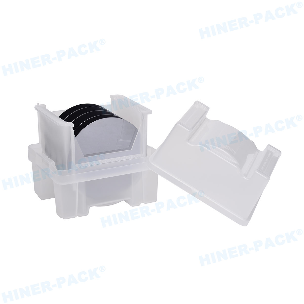
Third is mechanical precision. Trays are molded to tight tolerances with precise pocket dimensions. This ensures components are correctly aligned and prevents lateral movement during shipping. For wafer-level applications, trays may feature recesses that support the wafer’s edge without contact to the active surface.
Applications Across the Semiconductor Workflow
The utility of Gel Pak component trays spans the entire semiconductor lifecycle.
In Wafer-Level Packaging and Dicing, trays hold individual die after singulation. They are used for temporary storage before die attach or for shipping KGD to customers. The gel protects the active surface and prevents die “flipping” or bouncing.
For Multi-Chip Module (MCM) and SIP Assembly, different die from various sources are often kitted together. Using standardized trays ensures each fragile die is protected and easily identified until the pick-and-place machine retrieves it for assembly.
In Testing and Burn-In, devices must be securely held in sockets or carriers. Gel Pak trays act as a reliable interface, allowing automated handlers to pick devices from a known, safe location and place them into test sockets without manual intervention, increasing throughput and yield.
For Transport and Logistics, whether across a fab floor or across continents, these trays provide shock absorption, particle containment, and ESD protection. They stack securely and are often used within sealed, dry bags for moisture-sensitive devices.
Material Science and Customization by Hiner-pack
A one-size-fits-all approach fails in precision semiconductor handling. Hiner-pack specializes in tailoring its Gel Pak component trays to specific client needs.
This involves customizing the durometer (softness) of the gel. A softer gel may be used for extremely delicate, thinned wafers, while a firmer formulation might be better for larger, heavier packages.
Pocket layout and tray footprint are designed to match customer automation. Trays can be made to standard JEDEC outlines or custom sizes. Antistatic properties are calibrated to specific resistivity requirements, from fully conductive to static dissipative ranges.
Hiner-pack also focuses on cleanroom manufacturing protocols. Trays are produced and packaged in controlled environments to ensure they arrive as clean as when they left the factory, preventing them from becoming a contamination source.
Integration with Automation and Industry 4.0
Modern fabs and OSAT facilities are highly automated. Hiner-pack’s trays are designed for this reality. They feature precise fiducial marks for machine vision alignment and robust construction that withstands repeated robotic handling. The consistent release characteristics of the gel ensure high pick-and-place success rates.
Furthermore, trays can be designed with embedded RFID tags or barcode areas for full traceability. This allows each tray of components to be tracked through the supply chain, linking the physical handling container directly to digital logistics and inventory systems.
Conclusion: A Foundational Element for Yield Protection
In conclusion, the unassuming Gel Pak component trays are, in fact, a foundational technology for protecting yield and value in the semiconductor industry. They solve multiple critical problems—physical damage, particulate contamination, and ESD—in one elegant, passive system. For a trusted partner in developing these essential handling solutions, Hiner-pack combines material science expertise with deep semiconductor process knowledge. Their commitment to quality and customization ensures that whether you are handling advanced 5nm die or delicate photonic ICs, your components remain secure, organized, and protected from the fab to the final package.
Frequently Asked Questions (FAQ) About Gel Pak Component Trays
Q1: What exactly is the "gel" in a Gel Pak tray, and is it safe for bare silicon?
A1: The gel is a specially formulated, silicone-based polymer designed to be ultra-clean and inert. It is non-outgassing and will not transfer harmful silicones or other contaminants to sensitive device surfaces, making it entirely safe for direct contact with bare silicon, gallium arsenide, and other semiconductor materials.
Q2: How do I remove a component from the gel without damaging it?
A2: Components are removed using a standard vacuum pick-up pen or automated collet. The gel is designed for "easy release"—the suction hold is broken cleanly with vertical lift, requiring minimal force. No twisting or prying is needed, which prevents mechanical stress.
Q3: Can Hiner-pack's Gel Pak trays be used for long-term storage of devices?
A3: Yes, they are excellent for long-term storage when used correctly. For moisture-sensitive devices (MSD), the loaded tray should be placed inside a moisture barrier bag with desiccant. The trays themselves are stable and will not degrade or become tackier over time under normal conditions.
Q4: Are these trays reusable, and how do I clean them?
A4: High-quality trays from Hiner-pack are designed for multiple reuses. For cleaning, we recommend using compressed dry air or nitrogen to blow off loose particles. For more thorough cleaning, a lint-free wipe lightly dampened with isopropyl alcohol (IPA) can be used on the non-gel surfaces. Avoid soaking the gel in solvent.
Q5: Can you create custom tray layouts for non-standard component sizes or shapes?
A5: Absolutely. Customization is a key service at Hiner-pack. We can create trays with custom pocket sizes, arrays, and depths to fit unique die sizes, odd-shaped packages, or even partial wafers. The goal is to provide a perfect, secure fit for your specific components to minimize movement and maximize protection.


