
In the precise world of semiconductor logistics, a single static spark or a minute particle of dust can translate into millions of dollars in lost yield. Moving sensitive components like finished wafers, advanced logic die, or MEMS sensors between fabrication, testing, and assembly facilities presents a major risk point. Standard packaging often falls short, offering only basic physical protection or inconsistent static control. For engineers and supply chain managers, the solution lies in specialized, integrated systems designed for the highest level of security. Gel Pak anti-static boxes from Hiner-pack represent this category of purpose-built containers. They combine secure component immobilization with robust, multi-layer electrostatic discharge (ESD) protection, ensuring that sensitive devices arrive in the same condition they left the cleanroom.
Understanding the Threat: Beyond Basic ESD Bags
While metal-in static shielding bags are common, they have limitations for delicate, high-value items. Devices can move inside, leading to mechanical damage, chipping, or abrasion from friction-induced charging (tribocharging). Furthermore, bags alone do not prevent bending or crushing during transit.
A more rigorous approach is needed. This involves creating a stable, controlled micro-environment within the shipping container itself. The design philosophy behind Gel Pak anti-static boxes addresses this by eliminating internal movement and providing a Faraday cage effect against external ESD events.
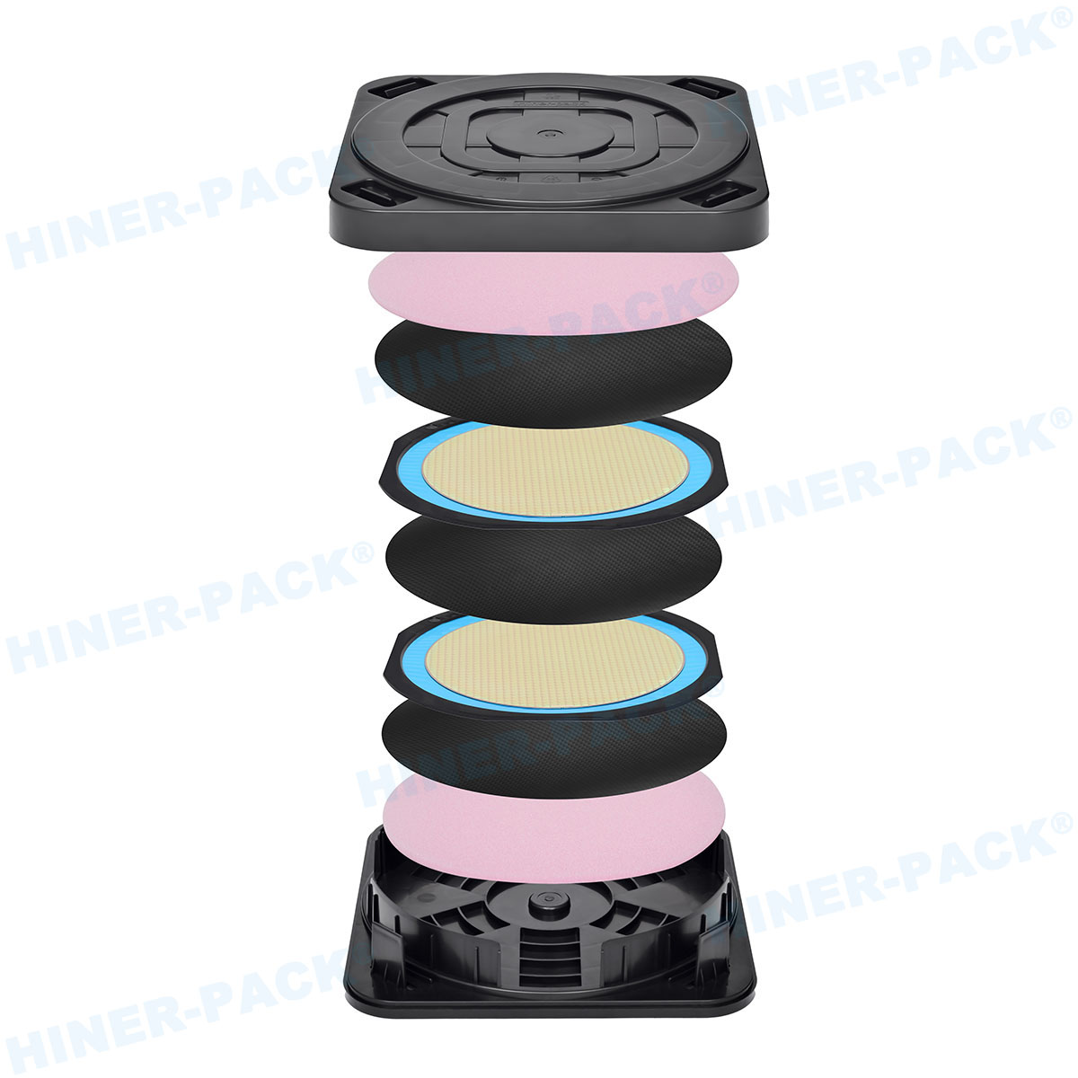
The Core Design: A Multi-Layer Shield
A Hiner-pack system is more than just a box. It is an integrated ecosystem of protection.
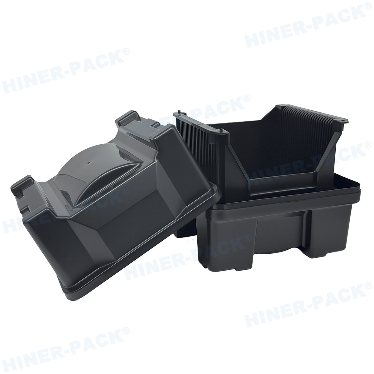
The foundation is the outer container. This is a rigid, durable box made from static-dissipative polypropylene or carbon-loaded composite materials. Its primary role is physical crush resistance and serving as the first line of static control.
Inside, the critical component is the custom-fit tray. This is often a conductive or static-dissipative plastic tray featuring the proprietary gel pad. This pad, with its precise tack level, holds each device or wafer firmly in place. This immobilization is the key to preventing in-transit damage.
Finally, a conductive lid seals the tray, and the entire assembly is placed inside the outer box. Some models include additional conductive foam or inserts for extra cushioning and to complete the Faraday cage, shielding contents from external static fields.
The Science of Secure Immobilization
The gel technology is what differentiates this system. The pad is not an adhesive; it is a hydrogel with controlled adhesion. It grips the backside of wafers or substrates securely without any chemical bonding.
This allows for safe, vertical lift-off using automated pick-and-place equipment or manual vacuum pencils, leaving no residue. By preventing any sliding or vibration, the gel also eliminates a primary source of particle generation and triboelectric charging during transport.
Material Integrity and Performance Standards
Hiner-pack materials are selected and tested for long-term reliability. The gel is formulated to be permanently static-dissipative. Its performance does not degrade over time or fluctuate with humidity levels, a critical factor for global shipments passing through varying climates.
All materials comply with key industry standards. This includes the ANSI/ESD S20.20 for ESD control and often meets JEDEC standards for tray dimensions and handling. Materials are also certified for low outgassing (tested per ASTM E595), preventing volatile condensable materials from contaminating sensitive device surfaces.
Primary Applications in the Semiconductor Supply Chain
These boxes are deployed where risk is highest and component value is greatest.
- Wafer-Level Shipments: Transporting fully processed wafers from a foundry to an outsourced assembly and test (OSAT) facility.
- Known Good Die (KGD) Distribution: Shipping tested, bare die to customers for multi-chip module or system-in-package integration.
- Sensitive R&D Sample Exchange: Protecting prototype devices and non-standard materials between research partners.
- Long-Term Storage of Critical Inventory: Providing a safe, static-free environment for high-value finished goods or legacy components.
Selecting the Right Hiner-pack Box Configuration
Choosing the correct system depends on specific device requirements and logistical needs.
Key considerations include:
- Device Sensitivity: The ESD sensitivity level (HBM, CDM) of the components dictates the required shielding level.
- Physical Dimensions: Boxes and internal trays are available in standard sizes (like 300mm wafer formats) or can be custom-designed for unique shapes.
- Stackability and Automation: Designs must integrate with existing warehouse racking and potentially with automated material handling systems (AMHS).
- Trip Duration and Conditions: For long-distance or international air freight, enhanced rigidity and climate consideration may be needed.
Hiner-pack’s Focus on Total Cost of Ownership
While the initial unit cost of a Gel Pak anti-static box system may be higher than a simple bag-and-bubble wrap approach, the total cost of ownership analysis tells a different story. By virtually eliminating in-transit damage and ESD failures, these boxes dramatically reduce the hidden costs of yield loss, rework, delayed shipments, and customer disputes.
The reusability of the robust outer box and, with proper inspection, the internal trays further enhances their economic value over multiple journeys. Hiner-pack works with clients to design systems that maximize this longevity and reliability.
For companies that cannot afford the risk of a compromised shipment, investing in certified, reliable packaging is a strategic decision. It safeguards not only physical assets but also brand reputation and customer trust. In an industry built on infinitesimal margins of error, the guaranteed protection offered by a well-designed Gel Pak anti-static box system is an essential component of a modern, resilient semiconductor supply chain.
Frequently Asked Questions (FAQs)
Q1: How do these boxes provide better ESD protection than a metal-in shielding bag alone?
A1: They offer multi-layer defense. While a shielding bag protects against external static fields, devices inside can still move, causing damage and tribocharging. The Hiner-pack system immobilizes devices on conductive gel, preventing movement-based charging. The rigid box also provides a physical Faraday cage, and the entire path from device to ground is controlled and permanent.
Q2: Can the internal gel trays be cleaned and reused?
A2: Yes, with proper procedure. The trays can be gently wiped with isopropyl alcohol (IPA) on a lint-free wipe to remove dust. The gel itself should not be soaked or scrubbed. Hiner-pack provides specific cleaning guidelines. Trays must be inspected for particulate contamination or gel degradation before reuse in a cleanroom environment.
Q3: Are these boxes compatible with common carrier shipping requirements and automated logistics systems?
A3: Absolutely. Hiner-pack designs boxes to meet standard dimensional and durability guidelines for major carriers. They can be barcoded and integrated into tracking systems. The rigid construction ensures stability on conveyor belts and in automated storage/retrieval systems (ASRS), unlike flexible bags.
Q4: Does Hiner-pack provide certifications for its materials, such as low outgassing?
A4: Yes. Upon request, Hiner-pack can supply standardized test data for key material properties. This commonly includes surface resistivity test reports per ESD STM11.11 and outgassing data per ASTM E595 (TML, CVCM). This documentation is often required for high-reliability aerospace, medical, or automotive semiconductor applications.
Q5: For a company new to this system, what is the typical implementation process?
A5: Hiner-pack typically starts with a consultation to understand your device specs, sensitivity, and logistics flow. They often recommend a pilot program with sample boxes for evaluation. Upon approval, they can scale production for standard or custom designs and provide handling procedure training for your warehouse and production staff to ensure correct usage.


