In the fast-paced world of semiconductor manufacturing, every square foot of cleanroom space is extraordinarily valuable. The relentless drive towards smaller, more powerful chips necessitates increasingly complex fabrication processes, which in turn require the careful handling and storage of more wafers than ever before. At the heart of this logistical challenge lies a critical solution: high-density wafer storage. This approach is not merely about stacking wafers closer together; it's a sophisticated integration of engineering, automation, and standards compliance designed to maximize space utilization, ensure wafer integrity, and streamline fab operations. This article delves into the core components of modern wafer storage, exploring the systems and standards that make it all possible.
The Critical Need for High-Density Wafer Storage in Modern Fabs
The economics of semiconductor fabrication are brutal. Building and maintaining a Class 1 or better cleanroom is one of the most significant capital expenditures a company can face. Therefore, maximizing the utility of every cubic meter of this controlled environment is paramount. Traditional open shelving or simple rolling carts are no longer viable for leading-edge fabs. They consume excessive floor space, increase the risk of contamination through human interaction, and lack the tracking capabilities needed for advanced process control.
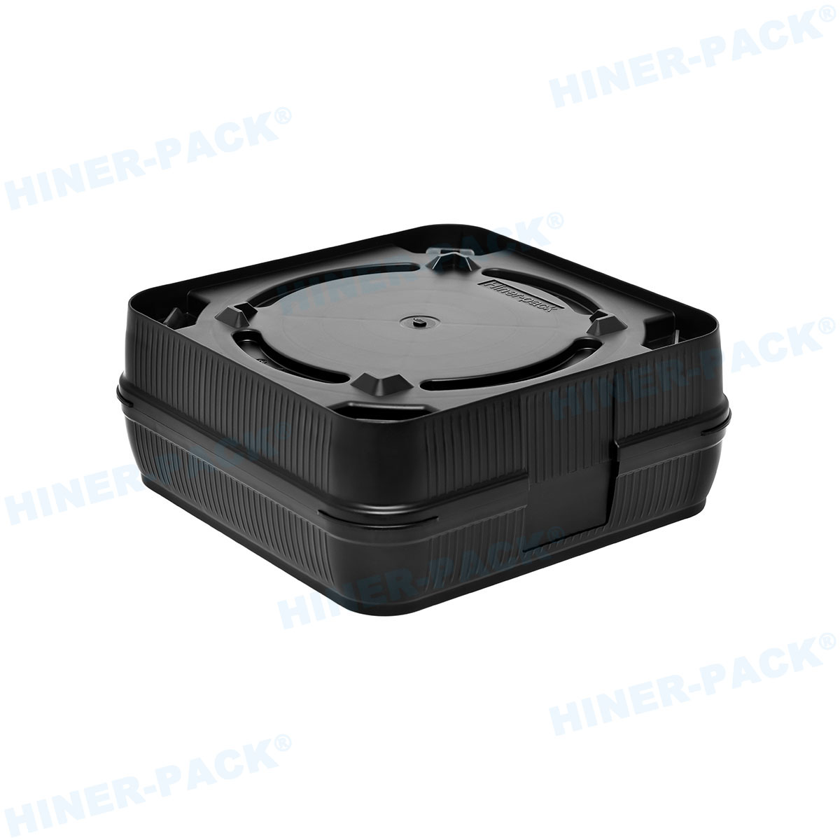
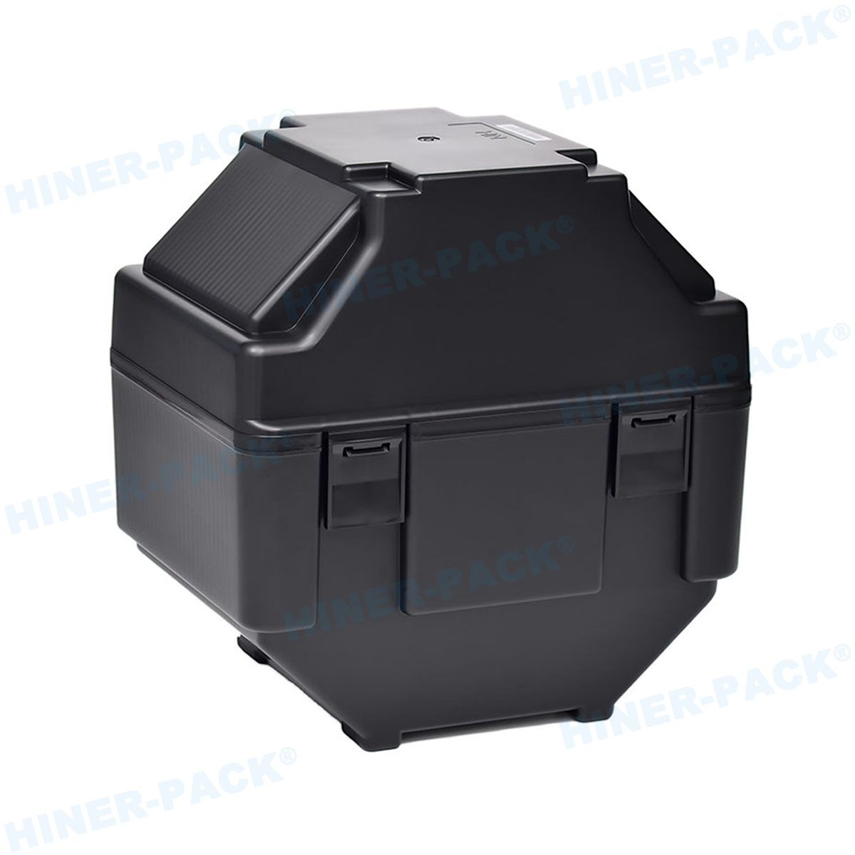
High-density wafer storage solves these problems by moving vertically. Instead of spreading out across the expensive cleanroom floor, these systems stack wafer containers—primarily Front Opening Unified Pods (FOUPs) for 300mm wafers—in dense configurations within a single footprint. This vertical integration can dramatically increase storage capacity by 200% to 400% compared to traditional methods, effectively freeing up precious cleanroom space for additional process tools or providing the necessary storage capacity within a smaller, less expensive facility. The benefits extend beyond mere space savings to include enhanced purity, improved inventory management, and faster throughput times.
The 300mm Wafer Storage System: Industry Standard for Automation
The shift from 200mm to 300mm wafers two decades ago was a watershed moment for the industry, fundamentally changing how wafers are handled and stored. The larger 300mm wafers are far too heavy and valuable to be handled manually without a high risk of damage and contamination. This necessitated the creation of a fully automated ecosystem, with the 300mm wafer storage system as its backbone.
A modern 300mm wafer storage system is built around the FOUP. This protective case is standardized to be handled precisely by automated material handling systems (AMHS), such as overhead hoist transports (OHTs) and automated guided vehicles (AGVs). The storage systems themselves are typically tall, enclosed structures that can be either cleanroom-compatible or located in a lower-class service bay. They interface directly with the AMHS, allowing FOUPs to be delivered, stored, and retrieved without human intervention. This seamless integration is the key to maintaining a continuous flow of wafers through the fab, minimizing queue times and ensuring tools are never idle waiting for a lot.
The Role of Automated Wafer Storage in the Smart Fab
Automated wafer storage is the engine of the modern "smart fab." It transcends the simple function of holding wOUPsp;it is an intelligent node in the fab's broader data and material network. When we talk about Automated wafer storage, we refer to systems like Automated Storage and Retrieval Systems (ASRS) or Stockers.
These systems are characterized by:
Robotic Handling: Internal robots (often a robotic arm or a telescopic fork) shuttle FOUPs between input/output ports and their designated storage locations within the unit.
Software Integration: They are managed by a Material Control System (MCS) that receives commands from the fab's Manufacturing Execution System (MES). The MCS knows the exact location of every FOUP, its contents, and its next destination.
Real-Time Inventory: The system provides real-time, accurate inventory data, eliminating manual tracking errors and providing complete lot traceability.
Contamination Control: By being enclosed, these systems protect wafers from airborne molecular contamination (AMC), particles, and fluctuations in temperature and humidity far better than open shelving.
The move to fully Automated wafer storage is a critical step towards the industry's goal of the "lights-out fab," a highly automated facility that can operate with minimal human presence.
Ensuring Interoperability: The Importance of SEMI Standard Wafer Storage
In an industry with equipment and parts supplied by hundreds of vendors worldwide, interoperability is non-negotiable. Imagine the chaos if every 300mm wafer storage system manufacturer used a different FOUP design or a unique port configuration. This is where the Semiconductor Equipment and Materials International (SEMI) standards come in.
SEMI standard wafer storage refers to systems and components designed and built in strict compliance with guidelines set by SEMI. These standards cover virtually every aspect of the storage and handling ecosystem:
FOUP Dimensions and Features: SEMI E47.1, E1.9, and others define the exact physical specifications, mounting points, and door mechanics of the 300mm FOUP.
Load Port Interface: SEMI E15.1 defines the critical interface between the AMHS/stocker and the process tool—the load port. This ensures a FOUP from any vendor can be presented to and accepted by any tool.
Carrier Kinematics: SEMI E58 defines the required positions and motions for reliable robotic handling of FOUPs.
SECS/GEM Communications: SEMI E5 (SECS-II) and E30 (GEM) standards govern how equipment communicates with host systems, ensuring the MCS can reliably control the Automated wafer storage system.
Adherence to SEMI standard wafer storage guarantees that a stocker from Vendor A will work flawlessly with FOUPs from Vendor B and OHTs from Vendor C, all controlled by an MCS from Vendor D. This interoperability protects fab investments and provides flexibility in sourcing equipment.
Planning Your Capacity: Utilizing a Wafer Storage Capacity Calculator
When planning a new fab line or expanding an existing one, accurately estimating storage needs is crucial. Underestimating leads to bottlenecks and operational nightmares, while overestimating leads to unnecessary capital expenditure. This is where a Wafer Storage Capacity Calculator becomes an indispensable tool.
A Wafer Storage Capacity Calculator is typically a software tool or a sophisticated spreadsheet model that helps engineers determine the optimal size and number of storage systems required. Key inputs into this calculator usually include:
Wafer Starts Per Month (WSPM): The volume of production.
Process Steps: The number of steps in the manufacturing process.
Process Time: The time each lot spends at each step, including queue time.
FOUP Capacity: How many wafers a single FOUP holds (e.g., 13 or 25 wafers).
Buffer Requirements: The amount of buffer stock needed to ensure smooth flow and account for equipment downtime.
By modeling the fab's workflow, the calculator outputs the required number of FOUP storage locations. This allows planners to select a 300mm wafer storage system with the right physical footprint and number of slots, ensuring the high-density wafer storage solution is perfectly tailored to the fab's specific needs before any equipment is purchased.
Common Challenges and Problems in High-Density Wafer Storage Systems
Even the most well-designed systems can face issues. Understanding these common problems is key to preventing them and ensuring reliable operation.
Robotic Handler Failures: The internal robot is the most complex mechanical part of an Automated wafer storage system. Jams, misalignments, or dropped FOUPs can bring storage operations to a complete halt, potentially damaging valuable product.
Software and Communication Errors: The storage system's integration with the MCS and MES is vital. Communication timeouts, database errors, or software bugs can cause the system to lose track of FOUPs or reject valid commands, disrupting material flow.
Load Port and Interface Issues: Misaligned guide pins, faulty latches, or failed sensors on the system's input/output ports can prevent a FOUP from being properly seated or transferred. Since these are SEMI standard wafer storage interfaces, maintenance is critical.
Contamination Control: While enclosed, stockers are not immune. Internal filters need regular replacement, and mechanical components can generate particles over time. Regular particle monitoring and preventative maintenance are essential.
Capacity Miscalculation: If the initial planning using the Wafer Storage Capacity Calculator was inaccurate, the fab can quickly run out of storage space, creating a major bottleneck that is expensive and disruptive to rectify.
Access Bottlenecks: In highly dense configurations, if multiple requests are made for FOUPs stored deep within the system, retrieval times can increase. Advanced software algorithms are needed to manage access and minimize delays.
High-density wafer storage is far more than a simple warehouse for silicon; it is a dynamic, intelligent, and absolutely critical component of a modern semiconductor fabrication facility. By leveraging automated 300mm wafer storage system technology built on a foundation of SEMI standard wafer storage, fabs can achieve unprecedented levels of efficiency, cleanliness, and space utilization. Careful planning with tools like a Wafer Storage Capacity Calculator ensures this infrastructure is right-sized for the job. While challenges exist, a well-maintained and properly integrated system provides the resilient backbone necessary to support the multi-billion-dollar operations that create the chips powering our digital world.


