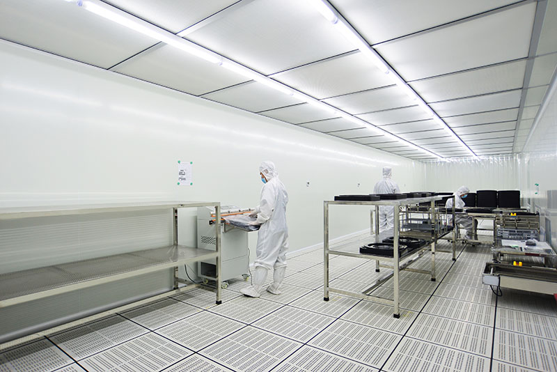
In the highly precise world of semiconductor manufacturing, the journey of a silicon wafer from fabrication plant to end-user is fraught with peril. The slightest jolt, shock, or vibration can render a multi-thousand-dollar wafer useless, leading to significant financial losses and production delays. This is where the science of impact-resistant wafer packaging becomes not just a logistical step, but a critical component of the entire supply chain. This article delves into the technologies and solutions, such as high durability wafer packaging and foam-in-place wafer packaging, that safeguard these delicate components, ensuring they arrive in pristine condition.
Why Impact-Resistant Wafer Packaging is Non-Negotiable
Modern semiconductor wafers, especially those fabricated for advanced nodes (e.g., 7nm, 5nm, and below), are incredibly fragile and susceptible to a multitude of threats. Microcracks, chipping, and latent damage caused by mechanical shock can compromise integrated circuits, leading to device failure. The primary goal of impact-resistant wafer packaging is to absorb and dissipate kinetic energy before it can reach the wafer itself.
This involves a meticulous engineering process focused on:
Shock Absorption: Converting the energy from a drop or impact into harmless heat through material deformation.
Vibration Damping: Mitigating the harmful effects of vibration during transportation, which can cause subtle but critical stress.
Contamination Control: Protecting wafers from particulate, molecular, and electrostatic discharge (ESD) hazards in addition to physical shock.
Without high durability wafer packaging, the yield losses incurred during shipping and handling could make the global distribution of semiconductors economically unviable.
Engineering High Durability Wafer Packaging: Materials and Design
The quest for high durability wafer packaging is a continuous process of innovation. It's not just about making a strong box; it's about creating a system that is both robust and precisely tailored to the delicate nature of its contents.
Key materials used include:
Engineered Polymers: Advanced polyethylenes and polypropylenes offer excellent strength-to-weight ratios and inherent shock-absorbing properties.
Rigid Plastics: Polycarbonate and ABS are used for creating sturdy outer shells and rigid wafer carriers (like FOUPs and FOSBs) that protect against crushing forces.
Composite Materials: Layers of different materials, such as plastic-aluminum composites, are used to create structures that are both lightweight and exceptionally strong.
The design philosophy revolves around creating a "package within a package." The inner system, often a foam-in-place wafer packaging solution or a pre-molded tray, cradles the wafer cassette, while the outer shell, or shock-resistant wafer shipper, bears the brunt of any external force. This multi-layer approach ensures that impacts are managed at every level.
The Precision of Foam-in-Place Wafer Packaging
One of the most effective methods for creating a custom cushioning system is foam-in-place wafer packaging (FIP). This process involves using specialized machinery to inject a two-part polyurethane foam into the void space between a wafer cassette and its outer shipping container.
The foam expands and cures within seconds, forming a perfect, rigid mold around the product. The benefits of this approach are significant:
Perfect Conformity: The foam expands into every crevice, creating a 100% custom fit that eliminates any movement inside the box. This is paramount for impact-resistant wafer packaging as it prevents the cassette from shifting during transit.
Superior Cushioning: The rigid foam has excellent energy-absorbing characteristics, effectively isolating the wafer from shocks and vibrations.
Cost-Effectiveness for Low Volume: While tooling for pre-molded trays can be expensive, FIP requires minimal tooling, making it ideal for low-to-medium volume shipments, prototypes, and high-value products.
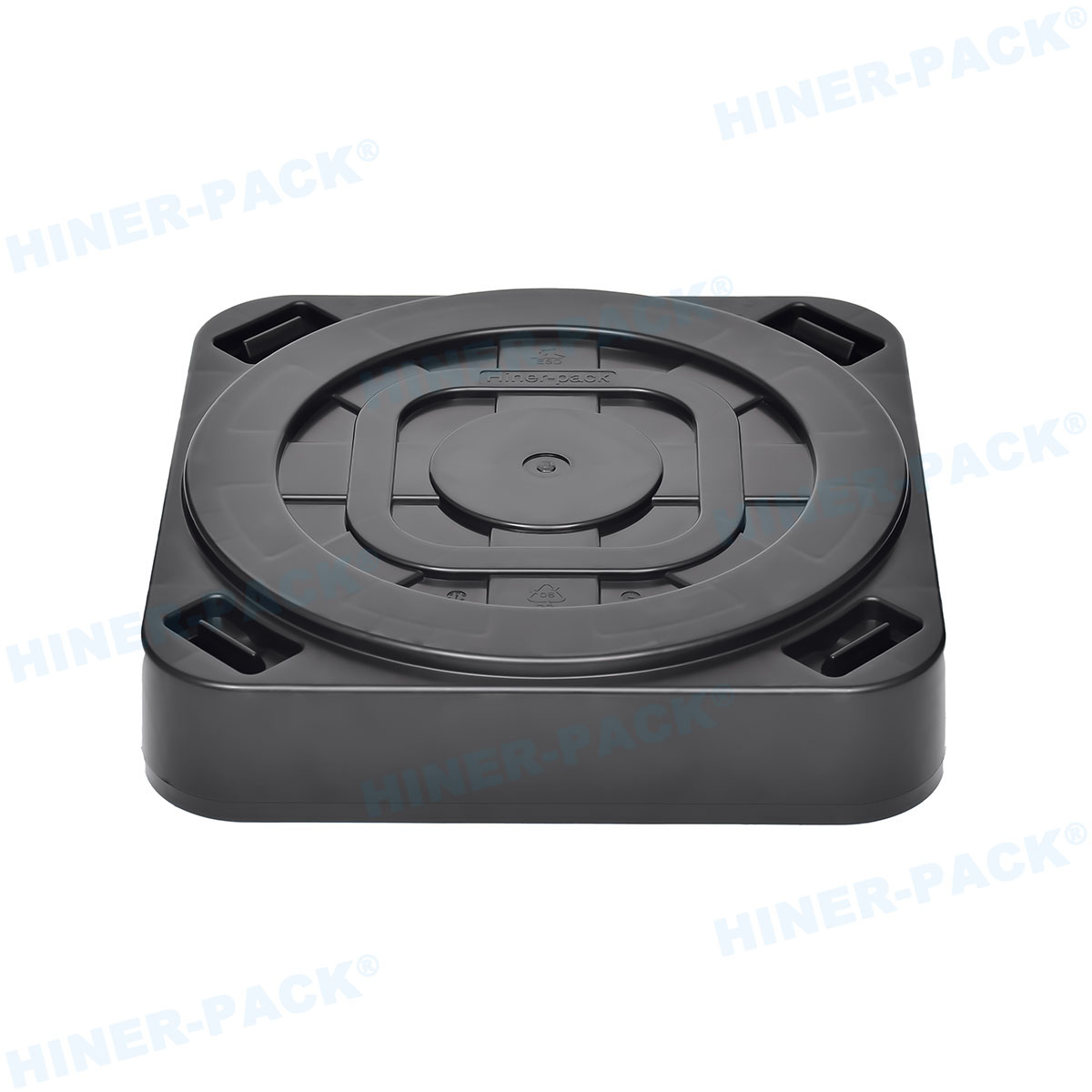
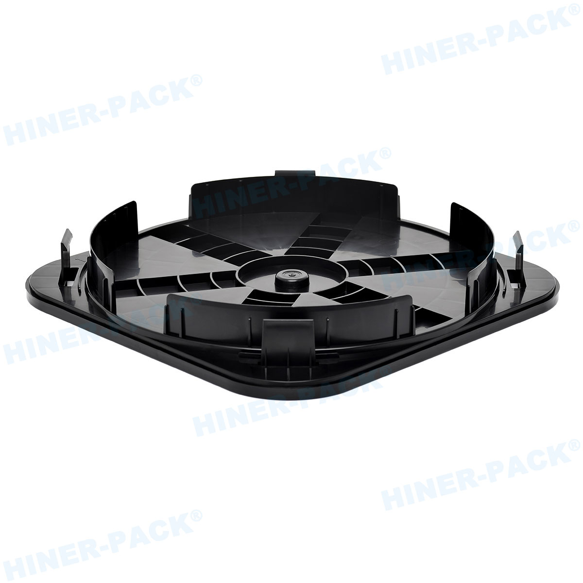
The Outer Shield: The Shock-Resistant Wafer Shipper
The first line of defense is the outer container, universally known as the shock-resistant wafer shipper. This is far more than a simple cardboard box. These are engineered containers designed to meet stringent industry standards, such as SEMI standards for wafer shipping.
A typical shock-resistant wafer shipper features:
Robust Construction: Made from durable, corrugated plastic or reinforced polymers that can withstand stacking and rough handling.
Standardized Sizes: Designed to accommodate standard 300mm and 200mm wafer cassettes (FOUPs and FOSBs) and interface cleanly with automated material handling systems (AMHS) in fabs.
Environmental Sealing: Many include desiccants and are designed to maintain a minimal internal environment, protecting wafers from humidity and airborne contaminants.
Certified Performance: They are rigorously tested to survive specific drop heights (e.g., 1-meter corner drops) and vibration profiles, ensuring reliable impact-resistant wafer packaging.
The Need for Custom Protective Wafer Packaging Solutions
While standard shippers exist, the diversity of wafer types, sizes, and sensitivity levels often demands a tailored approach. This is where custom protective wafer packaging solutions come into play. Not all wafers are created equal; a thin wafer for memory applications may have different requirements than a thicker power device wafer.
Custom protective wafer packaging solutions involve:
Risk Assessment: Analyzing the specific supply chain journey and identifying potential hazards.
Product-Specific Design: Creating packaging that accommodates unique wafer cassette designs or non-standard sizes.
Material Selection: Choosing the ideal foam density, polymer type, and structural design based on the fragility of the wafer and the expected logistics environment.
Validation Testing: Putting the custom solution through a battery of tests (drop, vibration, compression, climate) to certify its performance before full-scale deployment.
Investing in custom protective wafer packaging solutions is often a necessary step for manufacturers of cutting-edge or highly specialized components to ensure zero-fault logistics.
Common Challenges and Problems in Wafer Packaging
Even with advanced technology, several common problems can compromise the integrity of wafer packaging:
Material Fatigue: Repeated use of reusable shock-resistant wafer shippers can lead to wear and tear. Hinges may weaken, latches may break, and the structural integrity of foam can degrade over time, reducing its impact-resistant qualities.
Incorrect Foam Mixing: In foam-in-place wafer packaging, an inaccurate ratio of the two foam components can lead to incomplete curing. This results in foam that is either too soft (offering insufficient protection) or too brittle (which can crack and fail under impact).
Human Error in Packing: The effectiveness of foam-in-place wafer packaging is highly dependent on proper execution. Incorrect placement of the cassette before foam injection or using an expired foam cartridge can lead to packaging failure.
Contamination: Despite being high durability wafer packaging, if the materials used are not cleanroom-compliant (low outgassing, anti-static), they can introduce particles or molecular contaminants that ruin the wafers.
Inadequate Testing and Validation: Assuming a standard box will suffice without testing for a specific product's fragility can lead to disaster. Without proper drop and vibration testing, hidden weaknesses in the custom protective wafer packaging solutions may go unnoticed until it's too late.
Cost vs. Performance Trade-offs: There is constant pressure to reduce packaging costs. However, opting for cheaper, less robust materials often increases the risk of damage, leading to far greater costs in lost product and delayed production.
The safe transit of silicon wafers is a critical enabler of the global electronics industry. Impact-resistant wafer packaging is the unsung hero that makes this possible. Through the strategic use of high durability wafer packaging materials, the precise application of foam-in-place wafer packaging, the robust design of the shock-resistant wafer shipper, and the bespoke engineering of custom protective wafer packaging solutions, manufacturers can mitigate the risks of transportation.
Understanding and addressing the common problems associated with this packaging is equally important for maintaining high yield rates. As wafers become larger, thinner, and more valuable, the innovation in protective packaging will continue to be a vital field, ensuring that the heart of our digital world continues to beat reliably, no matter how far it travels.