
In the precise world of semiconductor manufacturing, every nanometer counts. Protecting delicate silicon wafers during transit, storage, and processing is not just a logistical step; it's a critical factor in yield preservation. This is where specialized packaging becomes as vital as the fabrication equipment itself. Among the most trusted solutions for this task are High-density waffle packs. These engineered containers provide a secure, organized, and contaminant-resistant environment for wafers, directly impacting production efficiency and cost. As demands for smaller nodes and higher throughput intensify, the role of robust packaging grows. Industry leaders like Hiner-pack have been at the forefront, refining the design and functionality of these essential components to meet the evolving challenges of fabs and OSAT facilities globally.
The Design and Functional Advantages of High-Density Waffle Packs
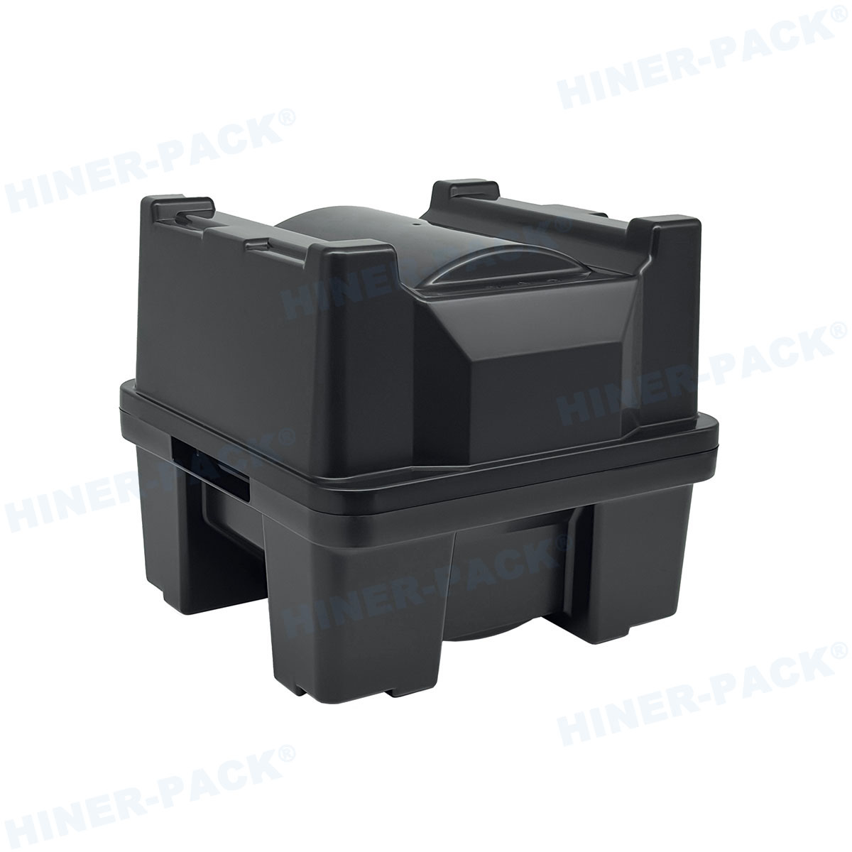
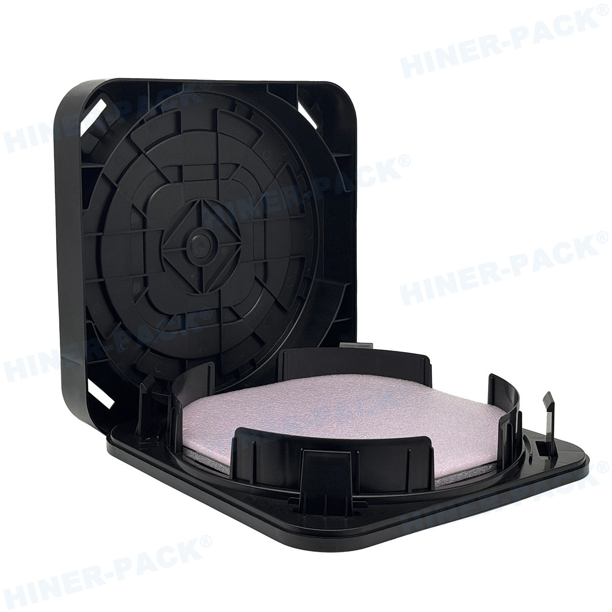
High-density waffle packs are not simple plastic boxes. They are meticulously designed trays featuring an array of individual pockets or cells, resembling a waffle pattern. Each cell cradles a single wafer, preventing contact and minimizing particle generation through friction.
The primary benefits of this design are clear:
- Physical Protection: The rigid structure and snug fit protect wafers from mechanical shocks, vibrations, and chipping during handling.
- Contamination Control: By isolating each wafer, the packs drastically reduce cross-contamination and in-transit damage caused by wafer-on-wafer contact.
- Process Efficiency: Standardized dimensions allow for easy integration with automated material handling systems (AMHS), robots, and processing tools. Operators can quickly load and unload wafers, speeding up workflow.
- High-Density Storage: As the name implies, these packs are optimized to hold many wafers in a minimal footprint. This is crucial for maximizing space in cleanrooms and storage facilities, where real estate is extremely valuable.
Material Science: Choosing the Right Polymer for the Job
The material composition of a high-density waffle pack is a science in itself. It must meet stringent requirements for purity, static control, and durability.
- Static-Safe Materials: Dissipative polymers, such as carbon-loaded PEEK or PC, are standard. They safely bleed off electrostatic charge, preventing electrostatic discharge (ESD) events that can destroy sensitive circuits.
- Low Particulate and Outgassing: Materials must be cleanroom-compatible, emitting minimal particles and chemical outgassing that could contaminate wafer surfaces.
- Chemical Resistance: Packs must withstand frequent cleaning cycles with harsh chemicals like IPA or specialized cleaning solutions without degrading.
- Thermal Stability: For processes involving temperature swings, materials must maintain dimensional stability to avoid warping that could trap or damage wafers.
Suppliers like Hiner-pack offer packs in various engineered polymers, allowing customers to select the optimal balance of properties for their specific process node and application.
Integration with Automated Handling and Front-Opening Unified Pods (FOUPs)
Modern semiconductor fabrication is highly automated. High-density waffle packs are designed to interface seamlessly with this automated landscape. Their standardized external dimensions (like common 300mm configurations) ensure they fit perfectly into load ports, overhead transport (OHT) vehicles, and storage racks.
A key interface is with the Front-Opening Unified Pod (FOUP), the sealed container that transports wafer lots between tools. Waffle packs are often loaded inside FOUPs, creating a dual-containment system.
- The FOUP provides a sealed mini-environment against airborne molecular contamination (AMC).
- The internal high-density waffle pack provides the structural organization and physical separation for the wafers.
This synergy is critical for maintaining wafer integrity through hundreds of process steps. Compatibility with these systems is a non-negotiable feature, and manufacturers design packs to meet or exceed SEMI standards for dimensional accuracy.
The Role of Trusted Manufacturers in Wafer Security
Choosing a supplier for high-density waffle packs is a decision with direct consequences for yield. Beyond simply molding plastic, a capable manufacturer provides consistency, innovation, and reliability.
- Precision Molding: Consistency in every cell depth and wall angle is paramount to ensure uniform wafer support and easy robotic pickup.
- Rigorous Testing: Packs should undergo thorough testing for ESD performance, particle shedding, and mechanical strength.
- Technical Support: Expert suppliers work with customers to solve unique challenges, whether for larger wafer diameters, fragile substrates, or specialized process integration.
Companies like Hiner-pack exemplify this approach, building their offerings on deep industry knowledge and a commitment to quality that meets the exacting standards of leading semiconductor producers.
Ensuring Longevity and Performance Through Proper Care
The performance of high-density waffle packs degrades with improper handling. Implementing a strict maintenance protocol extends their life and protects your investment in wafers.
- Regular Cleaning: Follow manufacturer-recommended cleaning procedures and intervals to remove accumulated particles and films.
- Careful Inspection: Each pack should be visually and functionally inspected before loading wafers. Look for cracks, warping, or wear in the cell structures.
- Proper Storage: When not in use, store packs in clean, sealed containers or in low-particle environments to prevent contamination.
- Adherence to Lifetime Cycles: Track the usage cycles of each pack. Even with the best care, polymers have a functional lifespan and should be retired before they become a risk.
In the grand scheme of semiconductor manufacturing, packaging might seem like a small detail. However, as wafer values skyrocket and geometries shrink, the margin for error vanishes. High-density waffle packs are a fundamental enabling technology, providing the safe, organized, and clean foundation that wafers require from fab to assembly. Their intelligent design directly supports automation, contamination control, and yield management goals. By partnering with experienced and quality-focused manufacturers like Hiner-pack, semiconductor companies can ensure that their most valuable assets are protected at every stage of the journey, turning packaging from a simple container into a strategic component for success.
Frequently Asked Questions (FAQs)
Q1: How often should high-density waffle packs be cleaned, and what methods are recommended?
A1: Cleaning frequency depends on your facility's cleanliness class and process steps. A common practice is cleaning after every process cycle or before loading a new, high-value lot. Recommended methods typically involve immersion or spray cleaning with deionized water and isopropyl alcohol (IPA) in a controlled environment, followed by drying in a particle-free oven. Always consult the pack manufacturer's guidelines, such as those provided by Hiner-pack, for specific procedures.
Q2: What is the typical wafer capacity for a standard 300mm high-density waffle pack?
A2: Standard 300mm packs commonly hold 25 wafers. This aligns with common lot sizes in fabrication. However, designs are available for different capacities, including 13-wafer or other configurations, to suit specific handling or process tool requirements.
Q3: Can high-density waffle packs be used for both prime and test/reclaim wafers?
A3: Yes, but it is a strong best practice to dedicate packs for one use or the other. Test and reclaim wafers can generate more particles and have a higher risk of contamination. Using separate packs prevents potential cross-contamination of high-value prime wafer lots.
Q4: How do I verify the ESD (electrostatic discharge) protection level of a waffle pack?
A4: Reliable manufacturers will provide certified test data for surface resistivity and resistance to ground, per standards like SEMI ESD-STM9.1 or ANSI/ESD S11.11. You can also perform periodic audits using surface resistance meters to ensure the pack's dissipative properties have not degraded over time.
Q5: Are custom designs available for unique wafer sizes or specialized applications?
A5: Absolutely. While standard sizes dominate, manufacturers often work with customers on custom solutions. This can include packs for non-standard wafer diameters (e.g., 150mm, 200mm), unique pocket designs for fragile compound semiconductor wafers, or specific features for MEMS or photonics applications. Discussing your needs with a supplier's engineering team is the first step.


