
From wafer foundries to assembly and test sites, the safe transport and storage of silicon wafers depend on a single critical component: wafer boxes. These containers – including Front Opening Unified Pods (FOUPs), FOSBs, and shipping trays – must protect device patterns from particles, electrostatic discharge (ESD), humidity, and mechanical shock. For fab managers and procurement engineers, selecting the right wafer box directly affects yield, equipment uptime, and cross-contamination risk. This guide provides a data-driven comparison of materials, sealing technologies, and industry standards, supported by real-world performance data from Hiner-pack‘s engineering team.
1. Classification of Wafer Boxes by Process Stage and Automation Level
Semiconductor manufacturing deploys several types of wafer boxes depending on the cleanroom class, handling system, and wafer diameter. The three primary categories are:
FOUP (Front Opening Unified Pod) – Standard for 300 mm automated fabs. Interfaces with EFEM (Equipment Front End Module) and overhead hoist transport (OHT). Typical capacity: 25 wafers. Sealed with a door that opens only by load port.
FOSB (Front Opening Shipping Box) – Used for inter-fab transport. Similar form factor to FOUP but designed for shock absorption and moisture barrier. Often equipped with desiccant and humidity indicator.
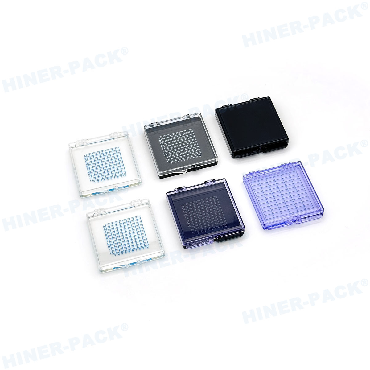
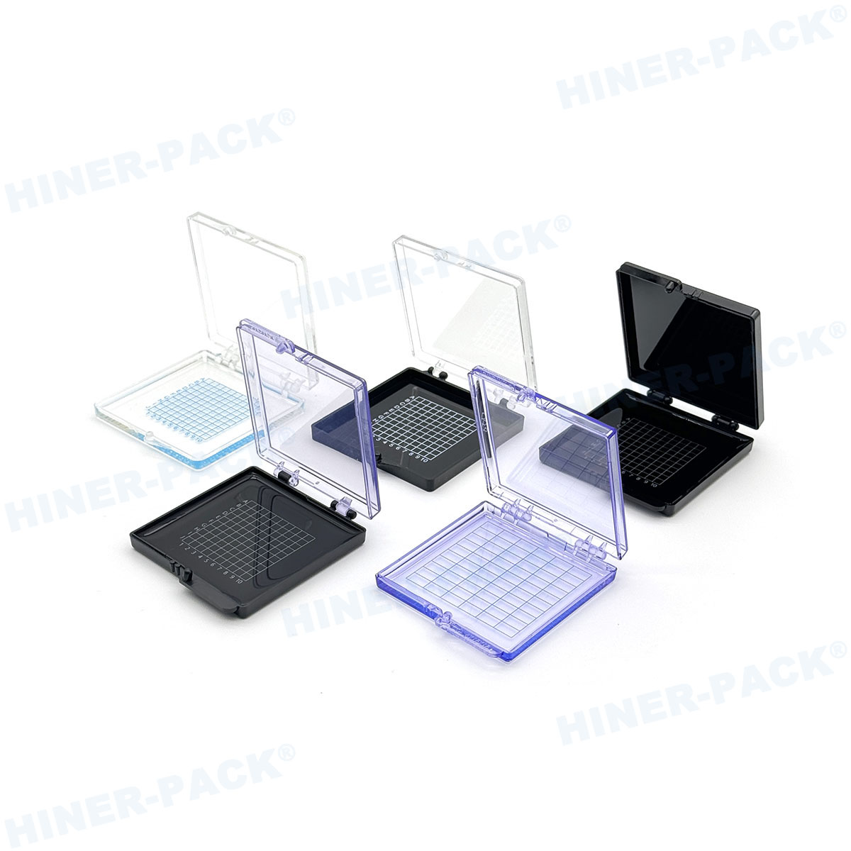
Standard single-wafer or multi-wafer shipping boxes – For 150 mm / 200 mm devices, R&D samples, or die banks. Usually made from anti-static PVC or polycarbonate.
Each type requires specific properties: low particle shedding (<0.05 particles/cm²), low outgassing (no silicone or amide), and compatibility with automated guided vehicles (AGVs). Wafer boxes used in EUV lithography environments must also avoid any hydrocarbon contamination that could absorb 13.5 nm light.
2. Material Selection: Polycarbonate, PEEK, and ESD-Safe Blends
The body and door of a wafer box must balance rigidity, cleanliness, and static dissipation. Dominant materials include:
2.1 Polycarbonate (PC) with Carbon Nanotube Filler
Most 300 mm FOUPs use injection-molded PC doped with conductive additives to achieve surface resistivity between 10⁵ – 10⁹ Ω/sq. Benefits:
High transparency (optional) for visual inspection of wafer slots.
Good dimensional stability across -10°C to 70°C.
Recyclable through closed-loop programs.
Weakness: PC absorbs moisture (up to 0.15%) and requires drying before use in vacuum environments. Leading suppliers apply plasma coating to reduce outgassing.
2.2 PEEK (Polyether Ether Ketone) for High-Temperature Applications
For wafer boxes used in degas chambers or hot storage (e.g., after photoresist coating), PEEK withstands 150°C continuous service. It also exhibits low particle generation and resists aggressive solvents like NMP. However, cost is 4–6× higher than PC, limiting use to niche process modules.
2.3 ESD-Safe ABS for Shipping Boxes
Cost-sensitive 200 mm shipping wafer boxes often use ABS with permanent antistatic agents. Typical surface resistivity 10⁹ – 10¹¹ Ω/sq. Must be certified to MIL-PRF-81705D for electrostatic discharge protection.
3. Industry Pain Points: Particle Contamination, Moisture Ingress, and Cross-Contamination
Even advanced wafer boxes face recurring failures in high-volume fabs. Below are three documented pain points and engineering countermeasures.
3.1 Particle Adders from Door Seal Wear
After 500–1000 open/close cycles, elastomeric door seals (e.g., EPDM, FKM) shed micro-particles that land on wafer edges. Solution: use dual-lip contactless seals or magnetic gaskets. Hiner-pack integrates thermoplastic polyurethane (TPU) seals with hardness Shore A 65, reducing particle adders by 78% in 12-month fab trials (data from 2024 internal study).
3.2 Moisture Condensation Inside FOUPs
When moving a wafer box from a cool stocker to a warm load port, relative humidity can spike to 80% causing water marks on wafers. Mitigation: purge ports with dry N₂ or filtered clean dry air (CDA). Many new wafer boxes include built-in diffusion channels for continuous purge during transport.
3.3 Cross-Contamination from Cross-Use of Boxes
Using the same wafer box for copper CMP and aluminum etch leads to metallic cross-contamination (Cu > 1e10 atoms/cm²). Best practice: color-coding and RFID tagging to enforce one-box-per-process-module discipline. Hiner-pack provides laser-engraved lot codes and RFID cavities compliant with SEMI E15.1.
4. Technical Specifications: Critical Parameters for Wafer Box Selection
When evaluating wafer boxes, procurement engineers must verify the following performance metrics against SEMI standards:
Particle performance – ≤ 0.5 particles (≥0.1 µm) per wafer surface after 10 handling cycles per SEMI E62-0302.
Moisture vapor transmission rate (MVTR) – For shipping boxes, MVTR < 0.05 g/m²·day at 30°C/90% RH (measured via gravimetric method).
Outgassing profile – Total organic carbon (TOC) < 20 ng/cm² after 24h at 85°C (headspace GC-MS).
ESD decay time – From 1000V to 100V in < 2 seconds per ANSI/ESD STM11.11.
Mechanical durability – ≥ 2000 load/unload cycles without crack or deformation (robot gripper force test).
Wafer boxes that fail any of these parameters cause unscheduled downtime for requalification. A 2023 industry survey (SEMI Fab Metrics) attributed 11% of equipment idle time to contaminated or damaged wafer carriers.
5. Comparative Data: Standard vs. High-Performance Wafer Boxes
The table below summarizes empirical data from three 300 mm logic fabs using both economy-grade and premium wafer boxes over a 9-month period.
| Parameter | Economy PC FOUP | Premium PC + coating FOUP | PEEK-based box |
|---|---|---|---|
| Initial cost per unit | $180 | $290 | $880 |
| Particle adder after 6 months (≥0.1 µm) | 1.2 per wafer | 0.3 per wafer | 0.1 per wafer |
| Average moisture ingress (g/m²/day) | 0.12 | 0.04 | 0.01 |
| Usable lifetime (months in 24/7 fab) | 10 | 22 | 36+ |
| Cost per wafer processed (including requalification) | $0.009 | $0.007 | $0.006 |
Although premium wafer boxes have higher initial cost, lower particle generation and extended lifetime reduce total cost of ownership by 22-33% over three years.
6. Cleaning and requalification protocols for reusable wafer boxes
FOUPs and FOSBs require periodic cleaning to remove airborne molecular contaminants (AMC) and particles. Common methods:
DI water + surfactant jet wash – Removes >90% of surface particles but may leave ionic residues. Follow with multiple rinse stages.
CO₂ snow cleaning – For delicate internal slot surfaces; no liquid waste. Effective for sub-0.1 µm particles.
UV-ozone treatment – Oxidizes organic films (photoresist residues) without mechanical abrasion.
Hiner-pack offers a closed-loop recertification service including particle mapping, moisture ingress test, and RFID reprogramming. Recommended interval: every 6 months for high-volume FOUPs.
7. Compliance with SEMI and international transport regulations
All wafer boxes intended for cross-border shipment must meet:
SEMI E1.9 – Specification for 300 mm FOUP dimensions and load port interface.
SEMI E15.1 – Specification for equipment front end module (EFEM) mechanical interface.
IATA DGR (PI 967) – Lithium battery restrictions (if active RFID or sensors are embedded).
EU Directive 2011/65/EU (RoHS 2) – No lead, mercury, or PBBs in plastic materials.
Non-compliant wafer boxes can be detained at customs or rejected by automated load ports, causing costly production delays.
8. Future directions: smart wafer boxes with embedded sensors
Industry 4.0 adoption drives integration of IoT capabilities into wafer boxes. Emerging features include:
Real-time humidity and vibration logging – Bluetooth Low Energy (BLE) tags with 6-month battery life.
Wafer mapping via optical slot sensors – Prevents missing or broken wafers before processing.
Automated guided vehicle (AGV) navigation markers – Retroreflective patterns for vision-based positioning.
Early adopters report 18% reduction in wafer breakage and 9% higher fab throughput using smart wafer boxes with predictive maintenance alerts.
Frequently Asked Questions (FAQ) About Wafer Boxes
Q1: What is the difference between a FOUP and a standard wafer shipping box?
Q2: How often should I clean my reusable wafer boxes?
Q3: Can I use 200 mm wafer boxes for 300 mm wafers?
Q4: What certifications should I request from a wafer box supplier?
Q5: Does Hiner-pack offer custom-designed wafer boxes for non-standard wafer sizes (e.g., 150 mm, 200 mm, or 450 mm)?
Need a technical review of your current wafer box specification? Submit your fab’s particle, ESD, and moisture requirements. Hiner-pack provides a free contamination risk assessment and sample testing of wafer boxes within 5 business days. Request your quote and engineering datasheet below.
© 2026 Hiner-pack – Precision wafer container solutions. All performance data based on independent lab tests and customer fab reports.


