
In semiconductor fabrication, wafer handling is critical for yield and efficiency. High-temperature wafer carriers play a key role in this process. They are specialized containers designed to hold silicon wafers during high-heat steps like annealing, diffusion, and chemical vapor deposition. This article explains their importance, design, and applications. We will also highlight Hiner-pack's expertise in producing reliable high-temperature wafer carriers for the global semiconductor industry.
What Are High-Temperature Wafer Carriers?
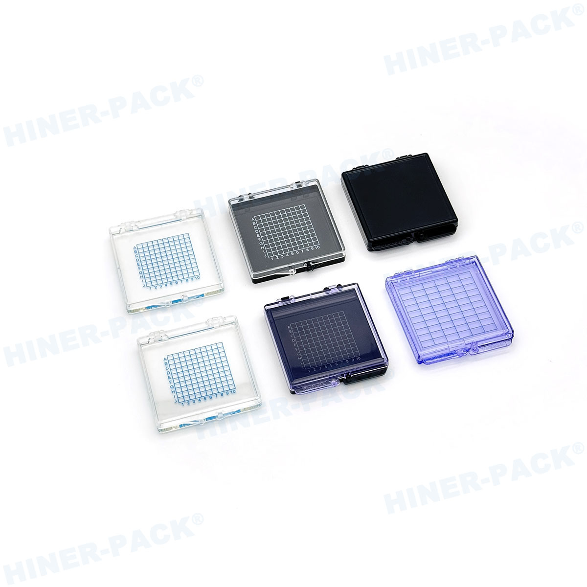
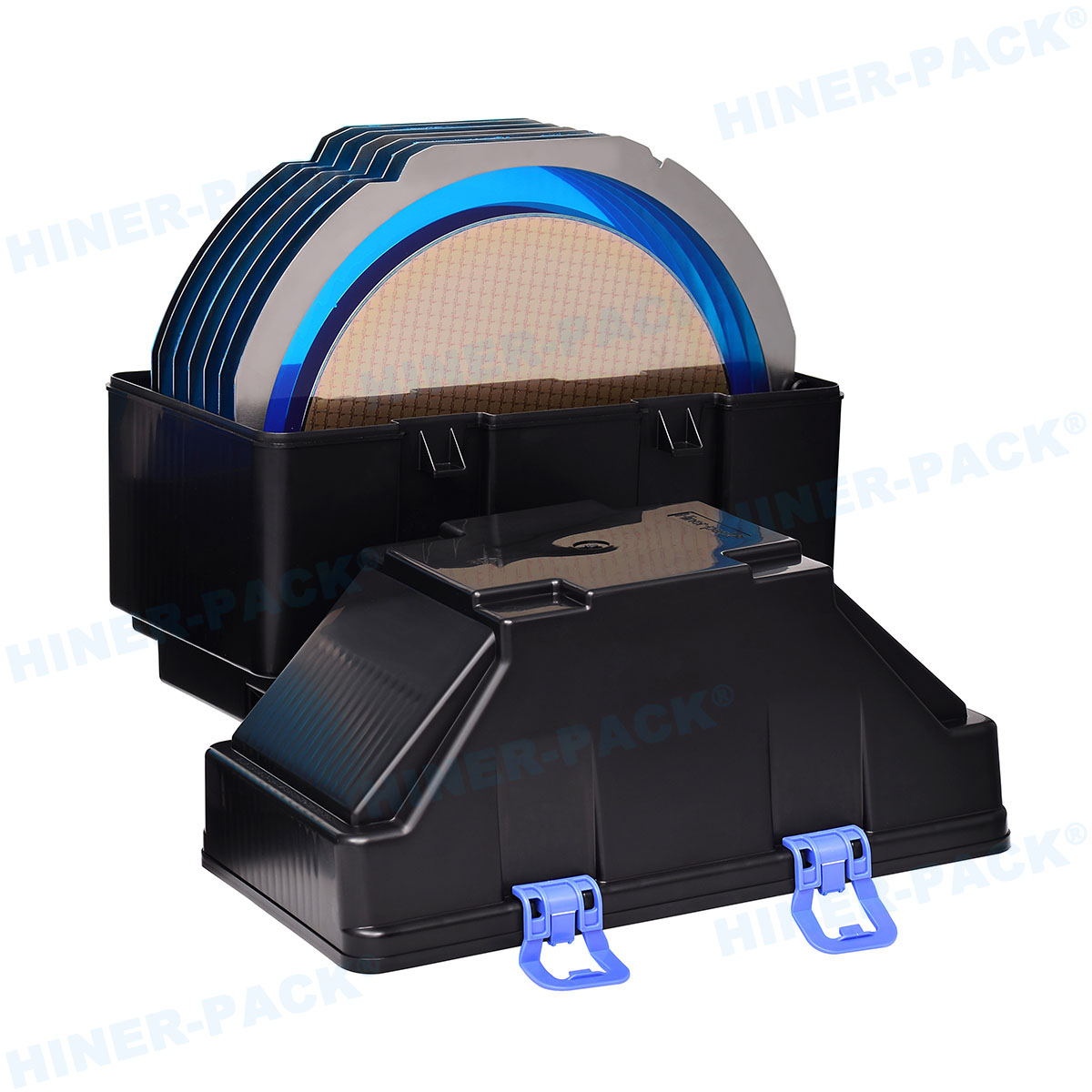
High-temperature wafer carriers are tools used in semiconductor plants. They transport and protect wafers in high-heat environments. These carriers must withstand temperatures above 1000°C without degrading. They ensure wafers remain clean and properly positioned. This reduces defects and improves production throughput.
Common types include boats, cassettes, and trays. They are used in furnaces and other thermal processing equipment. The design focuses on minimal contact to prevent contamination. High-temperature wafer carriers are essential for advanced node manufacturing.
Importance in Semiconductor Manufacturing
Semiconductor devices require precise thermal processing. High-temperature wafer carriers enable consistent heat distribution. This ensures uniform material properties on wafers. Without them, wafers could warp or collect particles.
Key benefits include:
Enhanced thermal stability during processing.
Reduced particulate generation at high temperatures.
Improved wafer alignment for automated systems.
Longer carrier lifespan, lowering operational costs.
The use of high-temperature wafer carriers supports scaling to smaller geometries. They are vital for memory and logic chip production.
Materials Used in High-Temperature Wafer Carriers
Material selection is crucial for performance. Carriers must resist heat, corrosion, and mechanical stress. The right materials prevent wafer damage and contamination.
Quartz and Fused Silica
Quartz is a common choice for high-temperature wafer carriers. It offers high purity and thermal shock resistance. Fused silica provides similar benefits with lower thermal expansion. These materials are suitable for oxidation and diffusion processes.
They are chemically inert and minimize metallic contamination. However, they can be brittle and require careful handling. Hiner-pack uses advanced quartz formulations for durability.
Silicon Carbide
Silicon carbide (SiC) is another key material. It has excellent thermal conductivity and strength. SiC carriers can handle temperatures up to 1600°C. They are often used in epitaxy and annealing steps.
SiC reduces particle shedding and extends carrier life. Its rigidity supports larger wafer sizes like 300mm. Hiner-pack integrates SiC in designs for demanding applications.
Design Considerations for High-Temperature Wafer Carriers
Design impacts carrier performance and wafer safety. Engineers focus on thermal management and cleanliness. Proper design ensures carriers function reliably in harsh conditions.
Thermal Stability
Carriers must maintain shape under thermal cycling. Warping can misalign wafers. Designs include slots and supports for even heat flow. Finite element analysis helps optimize structures.
Hiner-pack tests carriers in simulated furnace environments. This verifies stability across temperature ranges.
Contamination Control
Particles and impurities affect wafer yield. Carriers are designed with smooth surfaces and minimal edges. Coatings like silicon nitride can reduce outgassing. Regular cleaning protocols are essential.
Hiner-pack employs precision machining to limit debris. Carriers comply with SEMI standards for cleanliness.
Applications in the Semiconductor Industry
High-temperature wafer carriers are used in multiple fabrication steps. They support processes that define chip performance. Key applications include:
Thermal oxidation: Growing silicon dioxide layers on wafers.
Diffusion: Introducing dopants into silicon substrates.
Chemical vapor deposition (CVD): Depositing thin films.
Annealing: Repairing crystal defects after ion implantation.
Epitaxy: Growing crystalline layers on wafer surfaces.
In each case, high-temperature wafer carriers ensure safe wafer handling. They enable repeatable results across production batches.
Hiner-pack's Innovations in High-Temperature Wafer Carriers
Hiner-pack is a trusted brand in semiconductor components. We specialize in high-temperature wafer carriers for global clients. Our products combine material science with engineering expertise.
We offer customized solutions for specific process needs. Our carriers feature:
Advanced material blends for enhanced heat resistance.
Ergonomic designs compatible with automation tools.
Rigorous quality checks to meet industry standards.
Technical support for integration into existing lines.
Hiner-pack's high-temperature wafer carriers are used in fabs worldwide. They help manufacturers improve yield and reduce downtime.
Benefits of Using High-Temperature Wafer Carriers
Investing in quality carriers brings multiple advantages. They contribute to overall fab efficiency and product quality. Benefits include:
Higher wafer yield due to reduced contamination.
Lower maintenance costs from durable materials.
Improved process consistency for better chip performance.
Scalability to support next-generation wafer sizes.
Compliance with environmental and safety regulations.
Proper use of high-temperature wafer carriers minimizes rework. This speeds up time-to-market for semiconductor devices.
Future Trends in Wafer Carrier Technology
The semiconductor industry continues to evolve. Carriers must adapt to new challenges. Trends include:
Adoption of larger wafers like 450mm, requiring stronger carriers.
Integration of IoT sensors for real-time carrier monitoring.
Development of new materials for extreme temperature processes.
Focus on sustainability with recyclable carrier components.
Hiner-pack is researching these areas to advance high-temperature wafer carriers. We aim to support emerging technologies like 5G and AI chips.
High-temperature wafer carriers are indispensable in semiconductor manufacturing. They ensure wafers are processed safely and efficiently at high heat. From material choice to design, every detail affects fab performance. Brands like Hiner-pack provide reliable solutions that meet industry demands. As technology advances, the role of high-temperature wafer carriers will remain crucial for producing cutting-edge chips.
Frequently Asked Questions (FAQs)
Q1: What are high-temperature wafer carriers used for?
A1: High-temperature wafer carriers are used to hold and transport silicon wafers during high-heat semiconductor processes. These include annealing, diffusion, and chemical vapor deposition. They protect wafers from contamination and physical damage in furnace environments.
Q2: What materials are best for high-temperature wafer carriers?
A2: Common materials are quartz, fused silica, and silicon carbide. Quartz offers high purity and thermal shock resistance. Silicon carbide provides superior strength and temperature tolerance above 1500°C. The choice depends on the specific process requirements.
Q3: How do high-temperature wafer carriers prevent contamination?
A3: They are designed with smooth surfaces and minimal contact points. This reduces particle generation. Materials are selected for low outgassing and chemical inertness. Regular cleaning and coatings like silicon nitride further enhance cleanliness.
Q4: Can Hiner-pack customize high-temperature wafer carriers?
A4: Yes, Hiner-pack offers customized high-temperature wafer carriers. We tailor designs based on wafer size, process temperature, and equipment compatibility. Our team works with clients to develop carriers that meet unique fabrication needs.
Q5: How do high-temperature wafer carriers impact semiconductor yield?
A5: They directly impact yield by ensuring wafers are handled safely in high-heat steps. Proper carriers reduce warping, contamination, and misalignment. This leads to fewer defects and higher-quality chips, improving overall production efficiency.


