
Semiconductor manufacturing is a world of microscopic precision and relentless efficiency demands. As process nodes shrink and wafer sizes increase, manual handling becomes a bottleneck and a risk. This is where automated wafer carriers enter the picture. These systems are the silent, tireless workhorses moving delicate silicon wafers between tools. They eliminate human error, boost throughput, and safeguard multi-million-dollar production lines. For companies like Hiner-pack, designing reliable carrier solutions is central to modern fab operations. Understanding their role is key to grasping advanced manufacturing logistics.
Defining Automated Wafer Carriers
Automated wafer carriers are robotic or guided vehicles designed to transport wafer cassettes or FOUPs (Front-Opening Unified Pods). They navigate fab floors or overhead tracks without direct human intervention. Their core mission is safe, precise, and timely delivery. They interface directly with stockers, process tools, and metrology stations. This automation forms the backbone of the AMHS (Automated Material Handling System). Without them, 300mm fabs would struggle to function. Their continuous operation keeps production flowing 24/7.
Key Components and System Architecture
A complete system involves more than just the carrier itself. The vehicle, whether an OHT (Overhead Hoist Transport) or AGV (Automated Guided Vehicle), is one part. It includes a precision robotic arm or elevator mechanism for load/unload. The system relies on a network of tracks, rails, or guided pathways. A central control software, often integrated with the Fab’s MES, dispatches and routes carriers. Sensors and communication systems ensure collision-free navigation. Hiner-pack focuses on the carrier hardware that integrates seamlessly into this ecosystem. Reliability at this component level is non-negotiable.
Primary Functions in a Fab Environment
The functions extend beyond simple point-to-point movement. Automated wafer carriers enable just-in-time delivery of lots to tools, minimizing queue times. They manage buffer storage dynamically, optimizing floor space. They provide real-time tracking of wafer lots, feeding data into traceability systems. Crucially, they maintain the wafers in a controlled mini-environment, protecting them from particles. This orchestration of logistics is vital for achieving high tool utilization rates. Their performance directly impacts overall equipment effectiveness (OEE).
Main Types of Automated Transport Systems
Different fabs employ different solutions based on their scale and layout. Overhead Hoist Transport (OHT) systems are dominant in modern 300mm fabs. Carriers move on monorails above the cleanroom, saving floor space. Automated Guided Vehicles (AGVs) navigate defined paths on the floor, offering more layout flexibility. Rail Guided Vehicles (RGVs) are used for longer, point-to-point transfers between bays. Conveyor-based systems handle high-volume movements in specific zones. Hiner-pack’s expertise supports integration with these varied platforms, ensuring carrier compatibility.
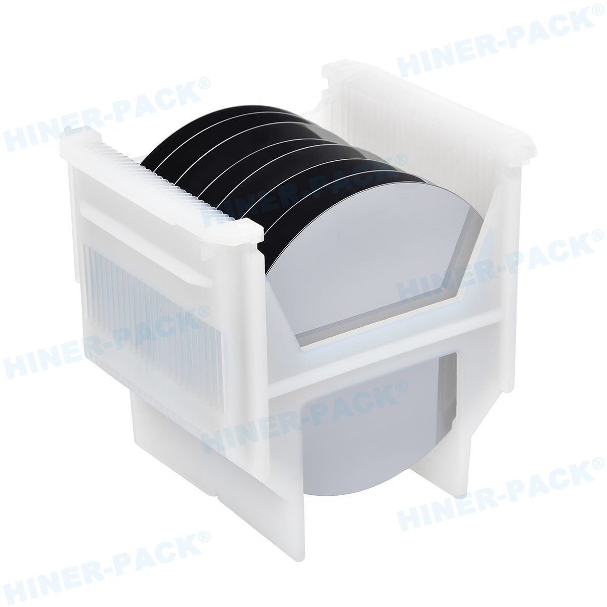
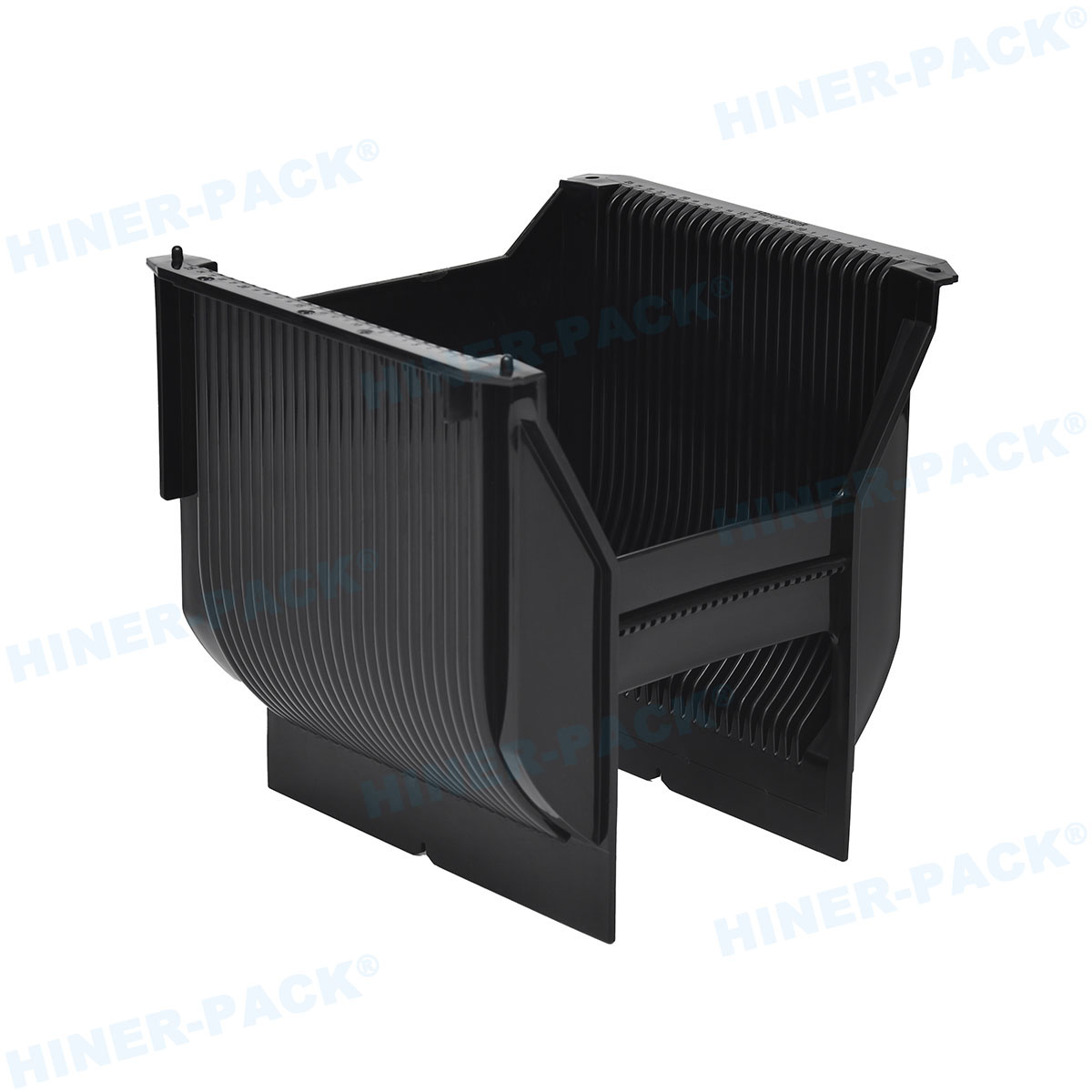
The Critical Link to FOUPs and SMIF Pods
The carrier and the pod are a paired system. For 300mm wafers, the FOUP is standard. Automated wafer carriers are engineered to grip, lift, and dock these pods with micron-level accuracy. The carrier’s mechanism must align perfectly with the FOUP’s docking plates and latching system. For older 200mm fabs, carriers handle SMIF (Standard Mechanical Interface) pods. This interface is where mechanical precision is paramount. A single misalignment can cause catastrophic misprocessing or wafer breakage. Hiner-pack designs carriers to master this interface consistently.
Material and Cleanroom Compatibility
Carriers must operate in stringent ISO Class 1-3 cleanrooms. Materials like anodized aluminum, stainless steel, and specialty cleanroom-grade plastics are standard. They must not outgas or generate particles. Lubricants are minimized or eliminated from moving parts. Designs favor smooth surfaces and rounded edges. Static control is also integrated to prevent electrostatic discharge. Hiner-pack selects materials that meet SEMI standards for cleanliness and durability, ensuring long-term reliability in harsh fab environments.
Integration with Fab Control Software
Intelligence is as important as mechanics. Automated wafer carriers receive commands from the Material Control System (MCS). They communicate their status, location, and any errors back in real time. This integration allows for dynamic rerouting in case of tool downtime or traffic jams. The carriers become data points in the digital twin of the fab. Hiner-pack ensures its carriers have robust and standard communication protocols (like SECS/GEM) for plug-and-play integration.
Hiner-pack’s Focus on Carrier Reliability
Hiner-pack approaches carrier design with a focus on uptime. Their components undergo rigorous lifecycle testing to simulate years of fab operation. Emphasis is placed on fail-safe mechanisms and easy maintenance access. They design for diagnostic simplicity, so technicians can quickly identify and replace a faulty module. This philosophy minimizes mean time to repair (MTTR). In an environment where minutes of downtime cost thousands, this reliability is a core value proposition.
Safety and Error Prevention Features
Safety is multi-faceted. Automated wafer carriers have multiple sensors: obstacle detection, load presence verification, and door status sensing. They include soft-stop and emergency brake systems. Anti-collision algorithms manage traffic on shared rails. From a process safety perspective, they prevent wrong lot delivery through barcode/RFID verification. Hiner-pack builds these layers of protection into their designs, safeguarding both the product and the personnel.
The Impact on Yield and Contamination Control
Every human interaction with a wafer lot is a contamination risk. Automated wafer carriers dramatically reduce this. They move pods in sealed environments. Their smooth, vibration-dampened motion prevents particle generation inside the FOUP. By ensuring consistent, gentle handling, they eliminate a variable that can affect defect density. For yield managers, a robust automated handling system is a foundational element of contamination control strategy.
Considerations for Retrofitting and Upgrades
Not every fab is greenfield. Retrofitting automation into an existing line is common. This requires careful analysis of floor space, tool interfaces, and workflow. Carriers for retrofit projects may need custom dimensions or lifting mechanisms. Hiner-pack often collaborates on such projects, providing carriers that bridge older tools with new automation standards. The goal is to achieve automation benefits without a complete fab rebuild.
Future Trends: Towards Greater Autonomy
The future points to smarter, more autonomous carriers. We see the integration of more onboard sensors for predictive maintenance. Machine learning algorithms will optimize routing in real-time beyond static rules. The concept of “lot-to-tool” matching could evolve with carriers having more decision-making logic. Interoperability between different OEM systems is also a growing focus. Hiner-pack’s development pipeline is aligned with these trends, preparing for the next generation of fab logistics.
Cost Justification and Return on Investment
The shift to automated wafer carriers requires significant capital. The justification lies in operational savings. Reduced wafer breakage and contamination directly protect revenue. Increased tool utilization through faster delivery boosts output. Labor can be redeployed to higher-value tasks. The data collected improves overall fab management. The ROI is calculated not just in cost savings, but in enabling the production of more advanced, valuable chips.
Why Automated Wafer Carriers Are Indispensable
The trajectory of semiconductor manufacturing is clear: larger wafers, more complex processes, and relentless cost pressure. Manual handling cannot meet the precision, speed, and cleanliness demands of this future. Automated wafer carriers have evolved from a convenience to an absolute necessity. They are the circulatory system of a modern fab. Partners like Hiner-pack, by focusing on robust and intelligent carrier solutions, help fabs achieve the seamless flow that cutting-edge production requires. Their continuous innovation in this space keeps production lines moving forward.
Frequently Asked Questions
Q1: What is the main difference between an OHT and an AGV in wafer handling?
A1: OHT (Overhead Hoist Transport) systems operate on fixed rails mounted on the cleanroom ceiling, maximizing floor space. AGVs (Automated Guided Vehicles) move on the fab floor using laser or magnetic guidance, offering more route flexibility but using floor space.
Q2: Can automated wafer carriers handle mixed sizes, like both 200mm and 300mm pods?
A2: Generally, carriers are dedicated to a specific pod type (e.g., FOUP for 300mm, SMIF for 200mm) due to precise mechanical interfacing requirements. Some advanced systems may use adaptive grippers or interchangeable load ports, but this is not standard.
Q3: How are collisions prevented in a busy OHT network?
A3: The control system (MCS) manages traffic using zone blocking and routing rules. The carriers themselves have onboard short-range sensors for obstacle detection. Sophisticated software creates virtual “bubbles” around each carrier and continuously optimizes traffic flow.
Q4: What kind of maintenance do these carriers require?
A4: Regular maintenance includes cleaning of sensors and rails, inspection of mechanical grippers and belts, lubrication of specified points with cleanroom-grade lubricant, and verification of communication systems. Hiner-pack provides detailed maintenance schedules for its equipment.
Q5: How long does it typically take to see an ROI after implementing a full AMHS with automated carriers?
A5: The payback period varies by fab size and volume but typically ranges from 1.5 to 3 years. The ROI comes from increased throughput, higher yield, reduced labor costs, and lower wafer damage. The exact calculation depends on the specific operational improvements achieved.


