
Every day, semiconductor fabs and assembly facilities handle thousands of wafers and delicate dies. The value packed into each silicon slice is immense. Even minor damage during storage or internal transport can wipe out weeks of intricate work.
Scratches, edge chipping, and electrostatic discharge are constant threats. Standard trays and containers often lack the specific protection needed for these high-value components. This is where dedicated Gel Pak storage solutions become a critical part of the production floor, not just the shipping department.
They offer a unique method of secure, static-safe containment. This article explores how integrating these systems from a trusted provider like Hiner-pack can directly protect your yield and streamline operations.
The Problem with Traditional Semiconductor Storage Methods
Many facilities use generic plastic trays or waffle packs for holding wafers and dies. These can present several risks.
Rigid plastic can allow components to shift during movement. This micro-abrasion creates particles and can lead to edge damage. Friction from sliding is a common source of contamination.
Static charge buildup is another major issue. Non-conductive materials can generate and hold charges. A sudden discharge can fry a sensitive die without any visible sign.
Furthermore, loose lids or open trays expose components to airborne dust and particulates. In a cleanroom environment, this undermines the entire controlled process.
How Hiner-pack Gel Technology Works for Secure Storage
The core of an effective system is the gel itself. Hiner-pack uses a proprietary, clean polymer formulation. It is designed for the semiconductor environment.
The gel is permanently tacky but non-transferring. It gently but firmly holds a wafer or die in place on its surface. This eliminates all movement within the container.
Think of it as a soft, static-dissipative anchor. The component sits perfectly still, whether the box is on a shelf or being carried across the room.
The gel is also non-outgassing. It will not release volatile compounds that could condense on the wafer surface. This chemical stability is verified for compatibility with sensitive processes.
Key Components of a Complete Gel Pak Storage System
A full Gel Pak storage solutions setup from Hiner-pack is more than just a single box. It is a coordinated system designed for workflow.
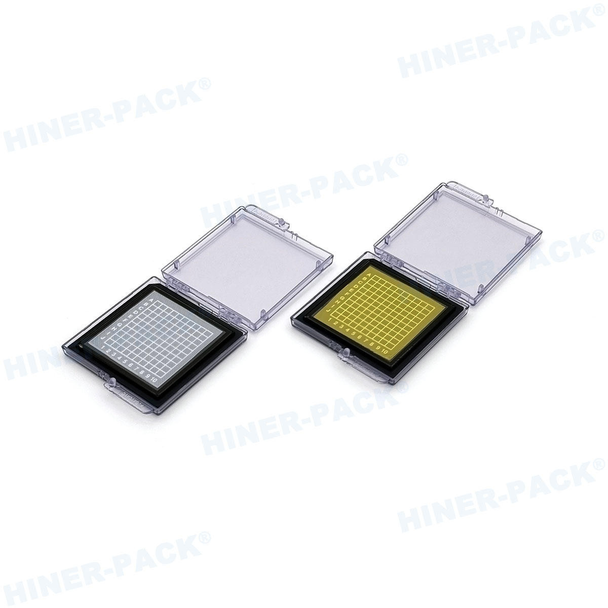
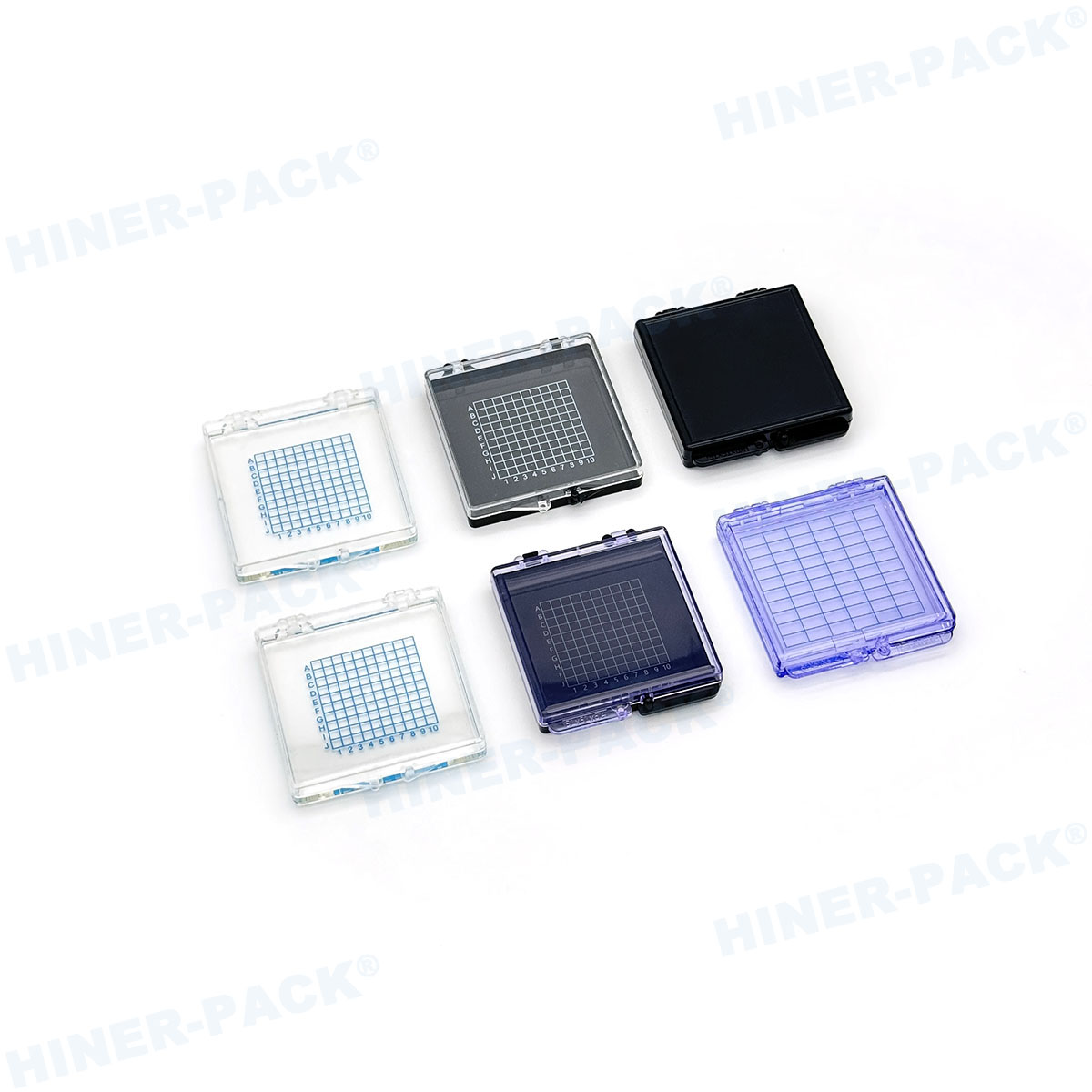
The foundation is the box or tray itself. These are made from static-dissipative polycarbonate or similar materials. They feature secure, positive-seal lids to create a micro-environment.
Inside, the gel is presented in different formats. Full sheets are for entire wafers or substrates. Pre-cut matrices hold individual dies in an organized grid, perfect for diced wafers or sorted chips.
Accessories include sturdy shelving units designed to hold the boxes securely. Transport carts allow safe movement of multiple stored units between workstations or cleanroom zones.
Labels and tracking software compatibility complete the system. Every box can be logged and traced, integrating with your MES (Manufacturing Execution System).
Application Scenarios on the Fab and Assembly Floor
Where exactly do these storage systems fit into the daily workflow? Their use cases are extensive.
In post-dicing, a wafer-on-tape is often placed directly into a Gel Pak tray. This holds it securely for short-term storage before the pick-and-place machine. It prevents tape relaxation and die shift.
For sample retention and failure analysis, components need safe, organized storage for days or weeks. A labeled matrix box provides perfect physical and traceability control.
Engineering teams use them to store prototype devices and test structures. The secure holding protects delicate bond pads and surfaces from contact damage.
In the assembly area, they are ideal for storing singulated dies before wire bonding or flip-chip attachment. The ESD-safe environment is crucial here.
Integration with Automated Material Handling Systems (AMHS)
Modern fabs rely on automation. The physical design of storage solutions must accommodate this.
Hiner-pack designs its storage trays with automation in mind. Standard exterior dimensions allow them to be picked up by automated guided vehicles (AGVs) or conveyor systems.
The low-profile, uniform design ensures reliable robotic handling. Boxes can be seamlessly transferred from storage shelves to process tools with minimal human intervention.
This integration reduces manual handling, which is a primary source of contamination and physical damage. It brings the protection of gel storage into the automated workflow.
Maintaining and Managing Your Storage System
To ensure long-term performance, proper maintenance is straightforward but essential.
The gel surface can be periodically cleaned to restore maximum tack. A lint-free wipe with high-purity isopropyl alcohol is typically used. Allow for full evaporation before reuse.
The boxes and lids should be cleaned with compatible solvents to remove particle buildup. Regular inspections for physical damage, like cracked lids or hinges, are recommended.
Implementing a rotation schedule for boxes ensures even wear. Tracking the lifecycle of each unit within your asset management system helps plan for gradual replacement.
Cost Considerations: Beyond the Initial Purchase Price
Viewing Gel Pak storage solutions as merely an expense misses the bigger picture. The true analysis is Total Cost of Ownership (TCO).
Consider the cost of a single ruined wafer due to poor storage. A few damaged dies can far exceed the investment in a fleet of protective boxes.
The reusability of Hiner-pack systems spreads the cost over years. They replace countless disposable trays and foam inserts, reducing recurring purchase orders and waste.
Indirect savings come from reduced downtime, fewer quality holds, and lower loss rates. Protecting your work-in-process inventory is a direct contribution to profitability.
Why Hiner-pack is a Partner for Your Storage Challenges
Selecting a supplier is about trust and reliability. Hiner-pack focuses specifically on the semiconductor and advanced electronics sectors.
Their product development is informed by direct feedback from process engineers. They understand the real-world challenges of cleanroom logistics and ESD control.
Quality is consistent from batch to batch. You can standardize across your global facilities with the assurance that every box performs identically.
Their technical support can help design custom matrix patterns or sizes for unique components. This level of partnership is crucial for specialized applications.
Conclusion: Building a Foundation of Protection
In semiconductor manufacturing, control is everything. You control the doping, the lithography, and the etching. It makes sense to extend that control to the storage and handling phases.
Implementing professional Gel Pak storage solutions from Hiner-pack brings that necessary level of control. It mitigates physical and electrostatic risks that older methods ignore.
The result is greater confidence in your process stability, lower hidden costs from damage, and a more organized, traceable workflow. It is an investment in the physical integrity of your product from fab to shipment.
Frequently Asked Questions (FAQs)
Q1: Can the gel damage the backside of a delicate wafer?
A1: No, when properly formulated like Hiner-pack's gel, it is non-abrasive and non-transferring. It provides secure adhesion without leaving residue or causing surface imperfections on silicon or compound semiconductors.
Q2: How long can components safely remain stored on the gel?
A2: For long-term archival storage (months to years), specific, low-migration gel formulations are recommended. For standard production floor storage (days to weeks), standard gels are perfectly suitable. Hiner-pack can advise on the best material for your duration.
Q3: Are these storage boxes compatible with nitrogen purge cabinets for sensitive devices?
A3: Yes. The materials are chemically stable and the seal of the lid is designed to be robust. Many customers successfully use Hiner-pack boxes within purge environments for added moisture protection.
Q4: What is the lead time for custom matrix patterns?
A4: Lead times vary based on complexity. Standard patterns may be readily available. For a new custom design, Hiner-pack typically provides a prototype within 3-5 weeks, followed by production scale-up. Early engagement is key for planning.
Q5: How do we validate the ESD performance of the storage system?
A5: Hiner-pack provides material certification sheets detailing surface resistivity and decay performance. You can also validate in-house using a static meter to test charge dissipation on received units, ensuring they meet your internal ESD program requirements.


