
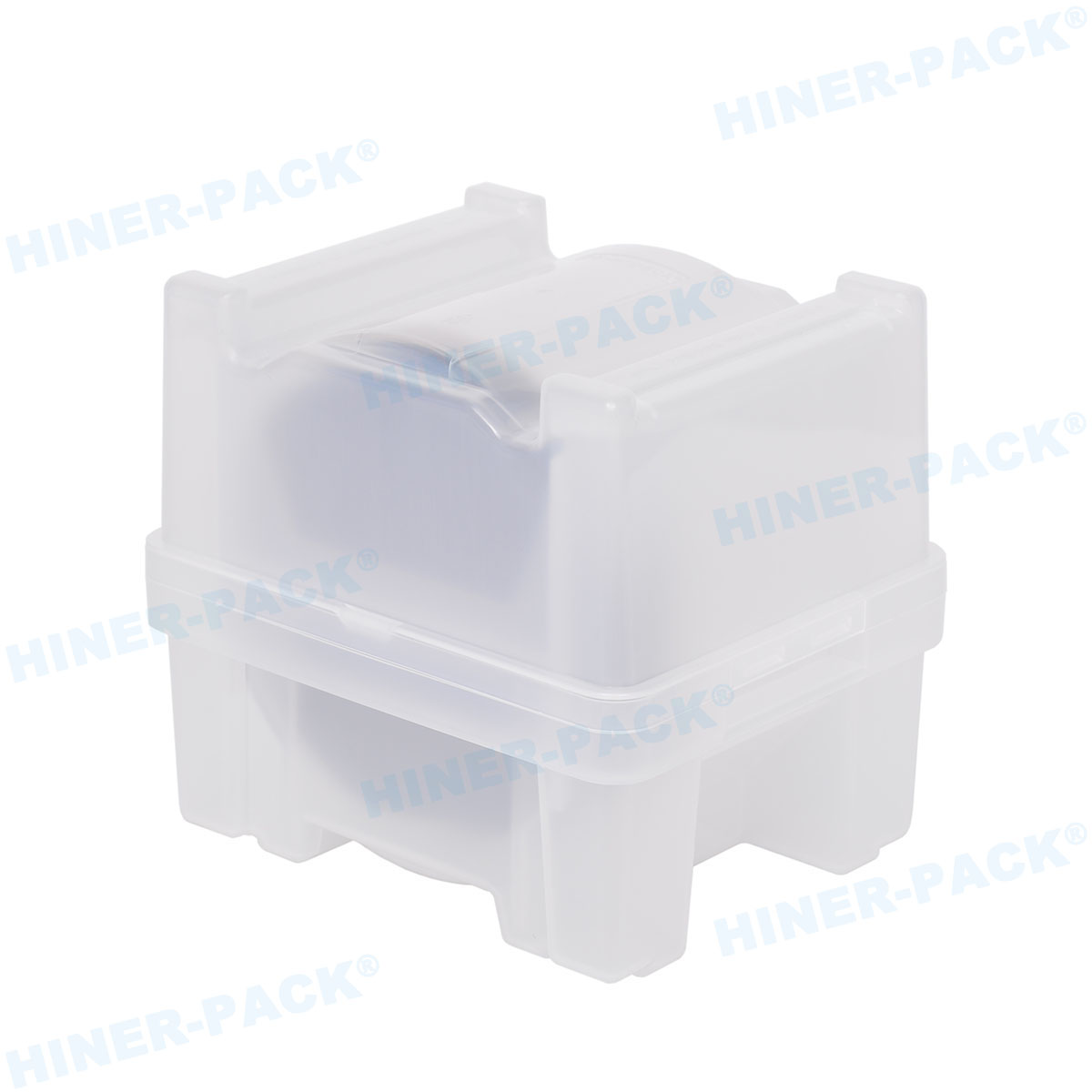
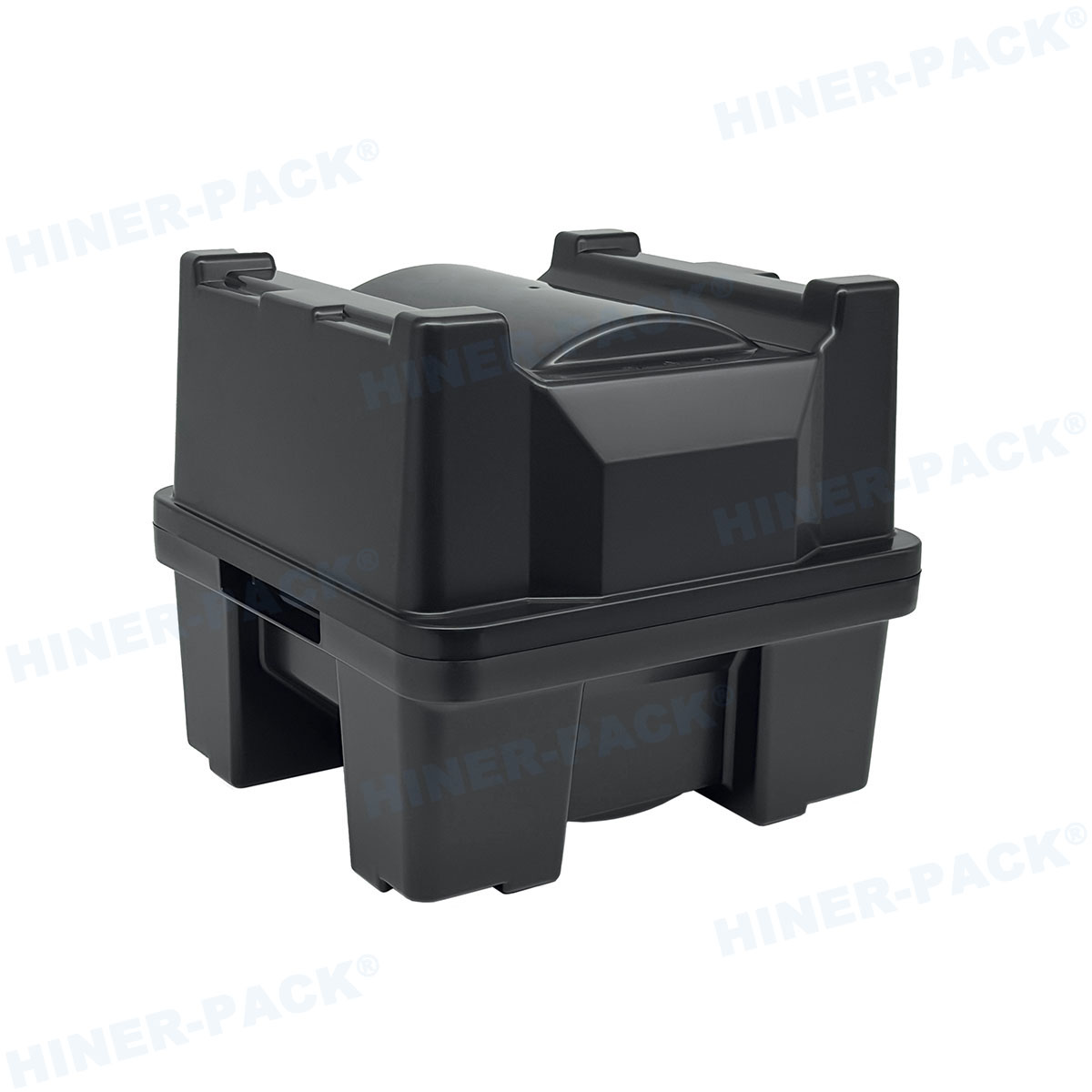
In the world of Very Large-Scale Integration (VLSI), the stakes are incredibly high. Billions of transistors are packed onto a single chip, and the margin for error is near zero. Beyond the complex lithography and etching tools, a critical yet sometimes underestimated component ensures these delicate wafers move safely through the fab: the VLSI wafer container. These are not simple boxes. They are highly engineered, precision micro-environments designed to shield valuable product from particles, molecular contaminants, and physical harm. The choice of container directly influences defect density, yield, and overall fab productivity.
The Non-Negotiable Battle Against Contamination
Contamination is the primary enemy in semiconductor manufacturing. For VLSI processes at advanced nodes, even a single microscopic particle can ruin multiple die.
Modern front-opening unified pods (FOUPs), the standard for 300mm wafers, function as mini cleanrooms. They maintain a constant, ultra-clean internal atmosphere through features like filtered purge systems. These systems gently flush the pod with inert gas or dry air, pushing out ambient particles and moisture.
The materials used must also be non-shedding. High-purity polymers like PBT or PC are engineered for low outgassing and low particle generation. This prevents the container itself from becoming a contamination source during transport and storage.
Material Science: More Than Just Plastic
The polymer selection for a VLSI wafer container is a science. It must balance mechanical strength, chemical resistance, and electrostatic discharge (ESD) properties.
Static charge can attract airborne particles like a magnet. Conductive or static-dissipative materials are integrated to safely drain charge, preventing particle attraction and dangerous electrostatic discharge that could damage sensitive circuits.
For specific processes, containers may need to withstand exposure to harsh chemicals or high temperatures. Suppliers like Hiner-pack develop specialized material formulations that meet these rigorous demands without compromising purity or dimensional stability.
Mechanical Precision and Automation Compatibility
In a fully automated fab, wafers travel for miles on overhead transport systems without human touch. The container must interface flawlessly with every tool, load port, and storage rack.
This demands extreme dimensional accuracy. Every kinematic coupling notch, handling flange, and door seal surface must be machined to micron-level tolerances. A misalignment can cause a tool jam, leading to hours of costly downtime.
The mechanical grip and the precision of the wafer slots are equally vital. Wafers must be held securely without stress or abrasion. Robotic end-effectors rely on the container's consistent internal geometry to pick and place wafers without error.
Managing the Internal Micro-Environment
A sealed container protects wafers, but it can also trap unwanted elements. Effective management of the internal environment is a key design focus.
Moisture is a major concern. It can lead to hazing, corrosion, and process defects. Desiccants or humidity-monitoring systems are sometimes integrated into container designs to maintain a dry state during extended storage or transport.
Pressure equalization is another detail. Rapid changes in atmospheric pressure can cause "pumping," forcing unfiltered air into the pod. Well-designed containers include breathable, filtered membranes that allow for pressure balance while blocking particles.
The Critical Role of Identification and Tracking
Traceability is paramount in a high-mix VLSI fab. Knowing the exact history and location of every wafer lot is essential for process control and quality assurance.
Containers are equipped with permanent data carriers, typically RFID tags or barcode labels. These tags store a unique ID and can log data like cycle count, last cleaning date, and process history.
This data integrates with the fab's Manufacturing Execution System. It allows for precise routing, prevents misprocessing, and enables predictive maintenance on the containers themselves. A supplier like Hiner-pack ensures their tags and mounting solutions are reliable and compatible with industry-standard readers.
Cleaning, Maintenance, and Total Cost of Ownership
A container is a long-term asset that undergoes hundreds of cycles. Its longevity and consistent performance impact total cost of ownership.
Regular, validated cleaning in dedicated washer tools is mandatory to remove accumulated films and particles. The container's design must facilitate this cleaning, with smooth surfaces and no fluid-trapping cavities.
Wear parts, like door seals and latching mechanisms, will eventually need replacement. A robust design with serviceable components extends the pod's operational life. Choosing a supplier with a strong global support network ensures access to spare parts and service expertise, minimizing asset downtime.
Conclusion: A Foundational Pillar of Fab Performance
In VLSI manufacturing, success is built on layers of precision and control. The wafer container is a foundational pillar in this structure. It is the guardian that ensures multi-million dollar wafer lots survive the journey from one Nobel Prize-winning process to the next.
Selecting the right VLSI wafer containers requires a partner who understands material science, precision engineering, and the day-to-day challenges of fab logistics. Companies like Hiner-pack focus on delivering this critical combination of reliability and performance. In the relentless pursuit of higher yield, the integrity of these containers remains an indispensable factor.
Frequently Asked Questions (FAQs)
Q1: What is the main difference between a FOUP and a simpler wafer cassette?
A1: A cassette is an open carrier that holds wafers in a process tool or during short-distance manual moves. A FOUP is a sealed, automated container with environmental controls. It is the standard for 300mm VLSI fabs, providing a mini cleanroom for wafers as they travel between tools and storage areas.
Q2: How often do FOUPs and other VLSI wafer containers need to be cleaned?
A2: Cleaning frequency is defined by the fab's contamination control strategy, based on monitoring data. It can range from every few cycles to after a set number of days in use. The schedule depends on the processes the container is exposed to and is often tracked automatically via the container's RFID tag.
Q3: Are there different VLSI wafer container designs for different processes?
A3: Yes. Standard containers are used for most lithography and etch steps. Specialized versions exist, such as "purge pods" for highly moisture-sensitive films, or containers with metal-sealed doors for processes that require an ultra-high vacuum or inert gas environment.
Q4: What industry standards govern the design of these containers?
A4: The SEMI International Standards organization sets the global benchmarks. Key standards include SEMI E47 for mechanical carrier specifications, SEMI E1.9 for dimensional tolerances, and SEMI E129 for RFID tag requirements. Compliance is essential for interoperability.
Q5: Why is the initial purchase price not the best indicator of a container's value?
A5: The total cost of ownership includes durability (cycle life), maintenance costs, compatibility (which affects tool uptime), and contamination performance (which directly affects yield). A slightly higher upfront investment in a robust, reliable container from a supplier like Hiner-pack often leads to significantly lower operational costs and higher overall yield.


