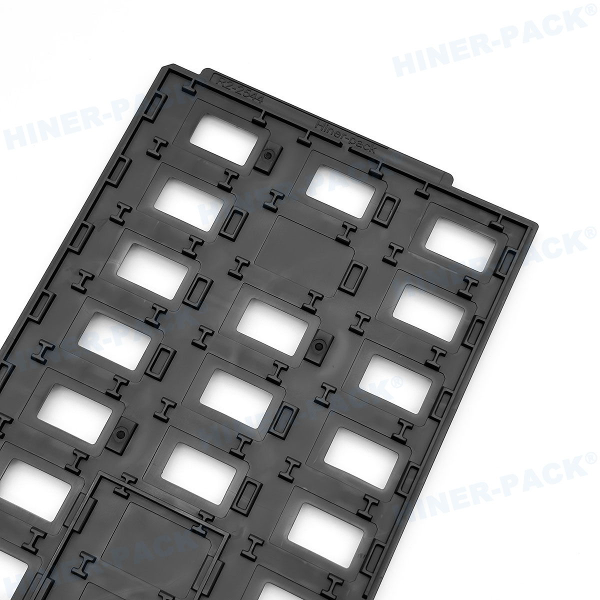
In semiconductor backend operations, the IC tray
cover is far more than a simple lid. It is a precision-engineered
component that directly impacts die integrity during storage, in-plant
transport, and international shipment. As device geometries shrink and package
types diversify — from QFN to complex 2.5D/3D stacks — the protective cover must
resolve electrostatic discharge (ESD) risks, mechanical abrasion, and airborne
molecular contamination (AMC). Hiner-pack, with two decades of JEDEC-compatible
tooling expertise, offers trays and covers that meet SEMI and ANSI/ESD S20.20
thresholds. This guide provides semiconductor engineers, procurement managers,
and OSAT quality teams with actionable data on IC tray
cover selection, failure mechanisms, and cleanroom
compatibility.
1. Critical Functions of an IC Tray Cover in the IC Supply Chain
The primary role of an IC tray
cover is to secure sensitive devices within a JEDEC or custom
carrier tray against three major risks:
Mechanical damage: During stacked tray handling, the cover
distributes vertical pressure evenly, preventing die chipping or lead
deformation.
ESD events: Without a properly grounded conductive cover,
tribocharging during sliding or separation can generate potentials exceeding
2kV, enough to damage gate oxides in advanced nodes (≤28nm).
Particle and moisture ingress: A tightly fitted cover with
optimized sealing ribs reduces particle ingress to <0.3 CFM (cubic feet per
minute) leakage, maintaining class 100 cleanroom integrity.
Leading IDMs and outsourced semiconductor assembly and test (OSAT) providers
report that switching from generic film lids to a rigid, ESD-safe IC
tray cover reduces handling-related defects by 60-75% (based on
internal 2023 yield audits).
2. Material Science & ESD Performance: Polycarbonate vs. PET vs.
Conductive Blends
Selecting the correct substrate for an IC tray
cover requires balancing surface resistivity, structural rigidity,
and outgassing limits. The table below summarizes industry-proven options:
Antistatic Polycarbonate (PC): Surface resistivity 10⁹–10¹¹
Ω/sq, high impact strength (Izod 12 kJ/m²), and temperature resistance up to
125°C. Ideal for burn-in board trays and automated handling.
Conductive Polypropylene (PP) with carbon fiber: Resistivity 10³–10⁵ Ω/sq, suitable for high-speed automated packing where rapid
charge dissipation is mandatory. Slightly lower flatness stability (±0.15 mm
over 300 mm).
PET-G with permanent antistatic agent: Lower cost for
single-use shipping covers, but prone to stress whitening and creep under
stacking loads >20 kg.
One often overlooked parameter is tribocharge generation when the cover
separates from the tray. Hiner-pack designs its IC tray
cover with a surface resistance gradient (10⁶–10⁹ Ω/sq on the inner
side and 10⁹–10¹¹ Ω/sq outer) to minimize charge separation while maintaining
non-slip stacking. Validated using a Faraday cup test per ESD ADV53.1.
3. Key Technical Specifications for High-Performance IC Tray Covers
Beyond material choice, five quantifiable metrics define a robust IC
tray cover:
Overall flatness (warpage): ≤0.2 mm over 300 mm length
(JEDEC tray standard). Greater warpage causes vacuum pickup failures in
automated die attach or test handlers.
Dimensional tolerance: ±0.05 mm for locking features and
peripheral ribs. Any deviation leads to “lid rocking” and uneven clamping
force.
Surface roughness (Ra): 0.4–0.8 µm to prevent particle
entrapment while allowing smooth robotic placement.
Cleanroom compatibility: Passes liquid particle count (LPC)
test per IEST-RP-CC004.3; no more than 50 particles >0.5 µm per 100 cm² after
ultrasonic cleaning.
Vibration resistance: Meets ASTM D4728 (random vibration)
for interstate and air freight, typically executed with 1.15 Grms for 60 minutes
without cover loosening.
Hiner-pack provides a certificate of conformance (CoC)
for every batch of IC tray covers, including profilometer
flatness readings and surface resistivity mapping. This traceability is critical
for automotive IATF 16949 audits.
4. Industry Pain Points and Engineered Solutions
Field returns from three major European assembly subcontractors reveal
recurrent failures tied to inadequate IC tray cover design:
Pain point: Warpage after autoclave reliability testing
(85°C/85% RH for 168h).
Solution: Use mineral-filled PC
compound with ≤0.1% moisture absorption. Hiner-pack cover
undergoes preconditioning (50°C dry bake for 4h) before shipment to
dimensionally stabilize the polymer.
Pain point: cover-to-tray locking failure during vibration,
causing ICs to escape pockets.
Solution: Redesign snap-fit
interference to 0.2–0.25 mm with draft angles of 3°. Finite element analysis
(FEA) verifies retention force >25 N per latch.
Pain point: Carbon black shedding from conductive covers
contaminating wire bond pads.
Solution: Co-injection molding
with a non-shedding core layer. Alternatively, use inherently dissipative
polymer (IDP) like poly(ethylene oxide) blended PC.
Pain point: High scrap cost due to lack of cover
reusability.
Solution: Implement closed-loop wash-and-return
program using deionized water + surfactant, followed by 100% optical inspection
for scratches. A well-maintained IC tray cover can survive 20
cleaning cycles without performance degradation.
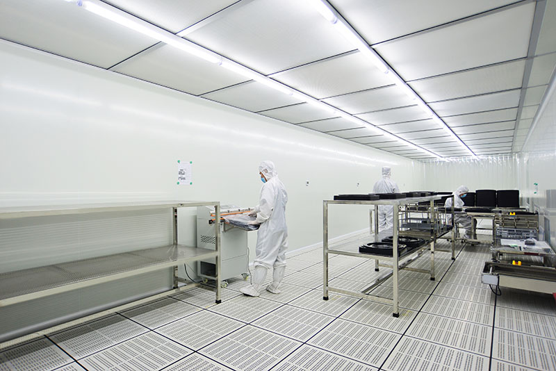
5. Cleanroom Integration and Reusability Lifecycle Management
For high-volume manufacturing fabs, the IC tray cover must
withstand automated depanelization and cleanroom robotic systems. The following
protocol ensures contamination control:
Incoming inspection: Every cover batch is sampled for
outgassing using GC-MS to detect siloxanes and plasticizers (target: no peak
>0.1 µg/g).
Washing parameters: Ultrasonic bath (40 kHz, 55°C) with 2%
alkaline detergent, followed by three rinses in 18 MΩ·cm DI water. Drying in
HEPA-filtered oven at 60°C for 2h.
Revalidation cycle: After 10 washes, measure surface
resistivity and flatness. Many standard covers fail after 12 cycles;
Hiner-pack designs for 25 cycles verified by internal extended
lifecycle testing.
Adopting a standardized cover management system reduces total cost of
ownership (TCO) by an average of 34% compared to single-use alternatives, as
shown in a 2024 SEMI packaging forum report.
6. Application Scenarios: From OSAT to IDM and Automotive Tier-1
Different environments demand tailored IC tray cover properties. Below are three real-world deployments:
Wafer-level CSP (WLCSP) handling: Requires ultra-low
particle generation (<200 particles >0.3 µm per cover).
Hiner-pack offers a polished nickel mold finish producing a
smooth cover surface; this reduces friction-induced particles by 45% compared to
standard EDM finishes.
Automotive power modules (IGBT trays): High stacking (up to
15 trays) mandates compressive creep resistance. A glass-reinforced PBT cover
with conductive filler maintains flatness under 5 kg per tray vertical
load.
RF / mmWave device shipping: Signal integrity demands
minimal dielectric interference; choose a cover with surface resistivity >10⁹
Ω/sq but with a grounded conductive path at tray corners to avoid floating-metal
antenna effects.
Customized tooling for non-JEDEC formats (e.g., 330x330 mm square trays) is
possible. Since 2019, Hiner-pack has delivered over 230 cover mold designs,
with lead times as short as 25 days for prototype tooling.
7. Supplier Evaluation Metrics: Beyond Price per Unit
When auditing potential IC tray cover vendors, competent
engineering teams focus on these indicators:
In-house simulation capability: Does the supplier perform
mold flow analysis to predict weld lines and sink marks that weaken latching
areas?
Metrology equipment: Look for Zeiss CMM or Keyence laser
micrometer for 100% inspection of critical dimensions.
ESD qualification data: Request charged device model (CDM)
discharge test results when the cover is attached to the tray. A well-designed
cover will not induce >250V peak on the IC leads during separation.
Environmental compliance: Full RoHS, REACH, and low-halogen
certificates. Many customers now require PFAS-free materials.
Hiner-pack maintains an ISO 17025-accredited lab for ESD and
cleanliness verification. Each cover delivery includes a digital lot record
accessible by QR code.
8. Conclusion: Improving Assembly Yield Through Engineered Cover
Strategies
Selecting a high-quality IC tray
cover directly influences first-pass yield, customer returns, and
automated handling uptime. Based on data from 14 semiconductor sites, migrating
from a poorly fitting or non-ESD cover reduces total defect per million (DPM)
from 3,200 to 850 on average. Key takeaways: always validate flatness after
temperature cycling, choose a material with documented tribocharge performance,
and demand batch traceability. For OSATs and IDMs planning tray reuse, partner
with suppliers like Hiner-pack that provide wash-validation services and
tooling modifications for friction minimization.
Frequently Asked Questions (FAQ) About IC Tray Cover
Q1: What is the difference between an IC tray cover and a standard
antistatic film lid?
A1: A rigid IC tray cover offers dimensional stability, uniform clamping force, and reliable stacking.
Films provide only dust protection and often wrinkle or tear under automated
handling, leading to misalignment. For high-value or fine-pitch devices, a rigid
cover is mandatory per SEMI G86-0321.
Q2: How many times can an IC tray cover be reused in a typical
cleanroom environment?
A2: With proper cleaning (DI water + mild
detergent, no ultrasonic over 45 min), a PC-based IC tray cover can be reused 15–25 times. Hiner-pack covers are tested for 25
cycles with less than 8% increase in surface resistivity. After each reuse,
inspect for cracks around snap-fits.
Q3: Can I get a custom IC tray cover for non-JEDEC
dimensions?
A3: Yes. While many trays follow JEDEC outlines (e.g.,
322 mm x 226 mm), Hiner-pack supports full custom design from 3D CAD.
Tolerances as tight as ±0.03 mm are achievable for alignment pins. Minimum order
quantity for prototypes can be as low as 50 units.
Q4: Which test standard verifies the ESD safety of an IC tray
cover?
A4: For covers, the key tests are ANSI/ESD STM11.11 (surface
resistivity), ESD STM11.31 (tribocharge from cover separation using a Faraday
cup), and IEC 61340-4-1 (charge decay time). Request the actual report, not just
a certificate. Acceptable decay time: <0.5 sec from 1000V to 100V.
Q5: How do I prevent IC tray cover warpage after steam aging
(85°C/85%RH)?
A5: Choose a cover resin with low moisture absorption
(<0.12% per ASTM D570). Additionally, request annealing: place covers in
120°C oven for 2h before first use to relax injection-molded stresses.
Hiner-pack pre-conditions all high-humidity covers,
guaranteeing warpage <0.25 mm even after 168h of 85/85 exposure.
Need a technical consultation or a quotation for your specific tray
format? Our engineering team provides sample evaluation, flatness
mapping, and ESD testing within 5 business days. Send your tray drawing or JEDEC
outline to Hiner-pack for a customized solution.
Request a quote or custom IC tray cover sample → Visit
our product page or contact our semiconductor packaging specialists. Click here for
inquiry and reference “tray cover deep dive” for priority
support.