In the precise world of semiconductor manufacturing, every component and process must be optimized for efficiency and safety. At the heart of handling and transporting finished integrated circuits (ICs) like QFPs, BGAs, and other surface-mount devices lies a crucial piece of packaging: JEDEC matrix trays. These standardized plastic trays are not just simple containers; they are engineered systems that protect valuable, sensitive components from physical damage, electrostatic discharge (ESD), and contamination throughout the supply chain. For engineers, procurement specialists, and operations managers, understanding the nuances of JEDEC matrix trays is essential for ensuring production line compatibility, minimizing yield loss, and streamlining logistics. This article delves into the specifics of these trays, their role in industry standards, and how partnering with a reliable supplier like Hiner-pack can simplify your packaging challenges.
Understanding the Foundation: What Are JEDEC Matrix Trays?
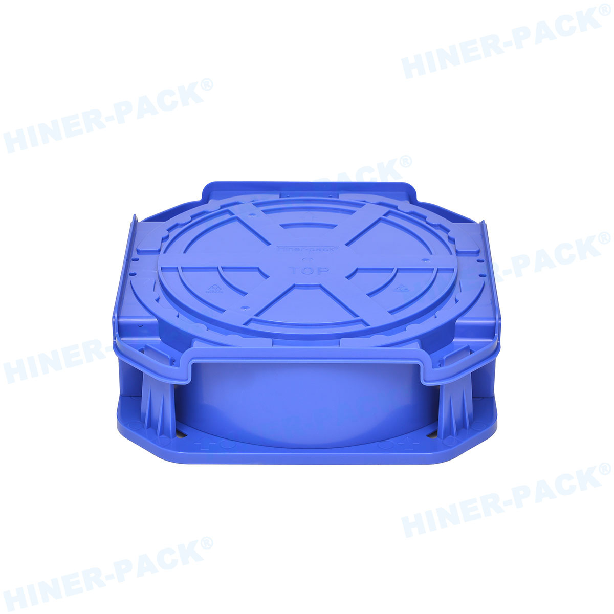
JEDEC matrix trays are rigid, rectangular trays designed with a precise array of pockets or cavities. Each pocket holds a single semiconductor device securely. The "matrix" refers to this organized grid pattern, which allows for automated handling, counting, and inspection. The "JEDEC" designation means the tray conforms to dimensional and material standards published by the JEDEC Solid State Technology Association, the global leader in microelectronics standards.
This standardization is the key. It ensures that a tray filled with chips at a fabrication plant in Asia will be perfectly compatible with the automated placement equipment at an assembly factory in Europe or the United States. Without JEDEC matrix trays, the industry would face chaos, custom tooling for every component shape, and significantly increased risk of damage.
A Brief History: The Evolution of Standardized IC Packaging
Before widespread standardization, semiconductor manufacturers and assemblers often used custom carriers or inefficient packaging like tubes and sticks for larger components. This led to compatibility issues, handling errors, and higher costs. Recognizing this bottleneck, JEDEC began developing and publishing formal outlines for tray dimensions in the late 20th century.
These standards, such as the well-known MO-048 for square trays and MO-220 for rectangular designs, defined everything from overall outer dimensions and thickness to the critical placement of tooling holes used by robotic handlers. The adoption of JEDEC matrix trays created a common language for IC packaging, accelerating automation and enabling the globalized, just-in-time production models that define the industry today.
Technical Specifications and Key Design Features
Not all matrix trays are identical. JEDEC matrix trays are defined by several critical specifications that users must understand for proper selection.
- Outline and Body Dimensions: Standards like MO-048 specify the exact outer length and width (e.g., 180.2mm x 166.0mm for a common size). This ensures they stack and fit into standardized magazines, racks, and shipping boxes.
- Pocket Configuration (Matrix Pattern): The number of pockets (e.g., 5x5, 6x6, 10x10) and their pitch (center-to-center distance) are precisely defined based on the component size they are designed to hold.
- Pocket Design: Pockets are engineered to securely cradle the device without applying stress to leads or solder balls. They often feature lead-in chamfers for easy insertion and retention lips.
- Tooling Holes and Notches: These are perhaps the most critical feature. Robotic arms use these holes to pick up and position trays with micron-level accuracy. Their location is non-negotiable for automation compatibility.
- Material and ESD Properties: JEDEC matrix trays are typically molded from static-dissipative or conductive materials like carbon-loaded Polycarbonate (PC) or Polyetheretherketone (PEEK). This safely drains any static charge, protecting devices from potentially catastrophic ESD events. Hiner-pack offers trays in a range of ESD-safe materials tailored to different environmental and durability needs.
Primary Applications in the Semiconductor Supply Chain
The use of JEDEC matrix trays spans the entire lifecycle of a semiconductor device.
- Final Test and Inspection: After wafer dicing and assembly, individual chips are placed into trays for electrical testing and optical inspection.
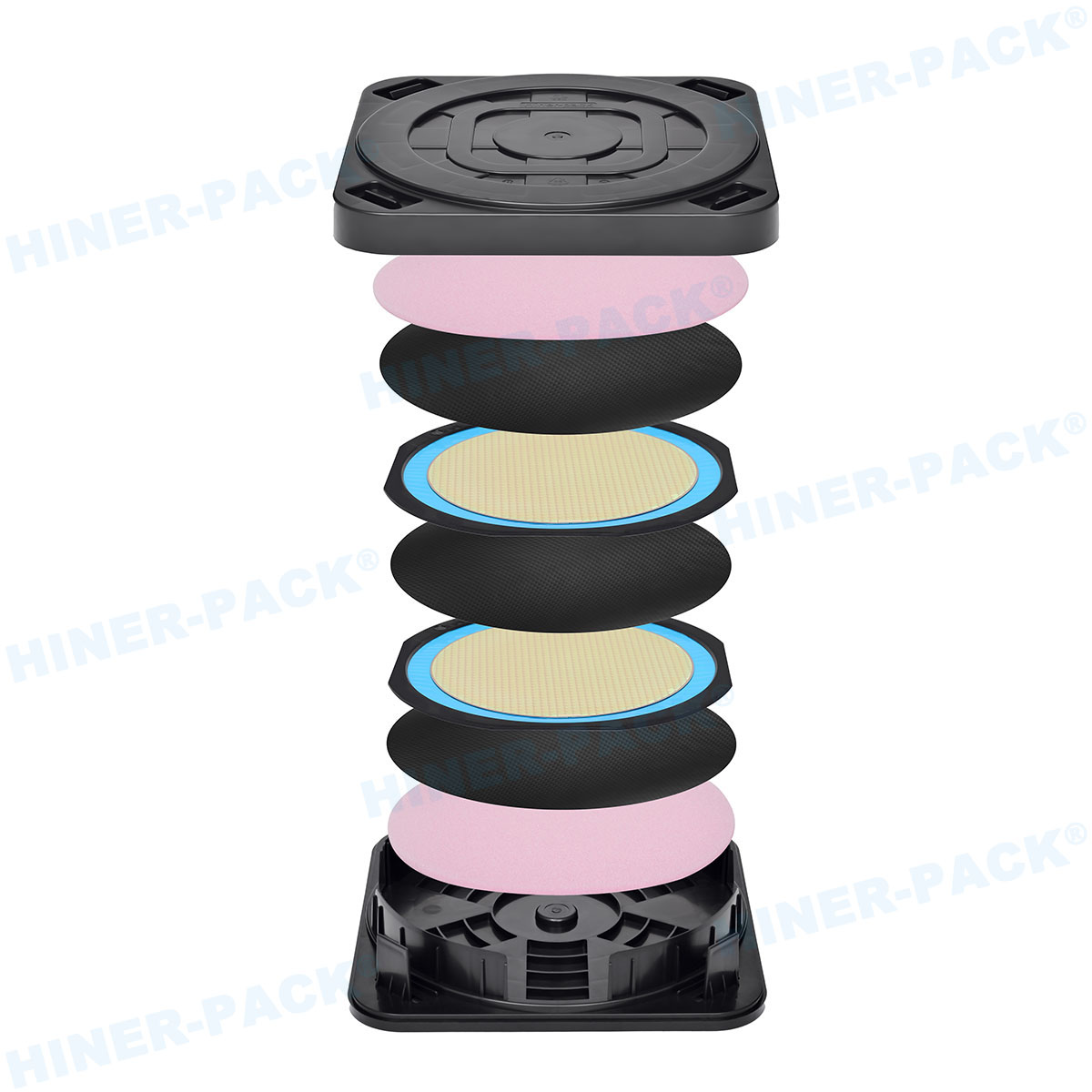
- Transport and Storage: Trays provide safe, organized storage and are stacked in magazines for transport between facilities or to distributors.
- Automated PCB Assembly: At the contract manufacturer (CM), automated equipment picks components directly from the standardized trays and places them onto printed circuit boards. This is where compatibility is paramount.
- Handling of Sensitive Components: High-pin-count and fine-pitch BGAs rely on trays to protect their delicate underside solder balls from damage or contamination.
Selecting the Right JEDEC Matrix Tray: A Practical Guide
Choosing the correct tray involves more than just matching component size.
- Refer to the Component Outline Drawing: Always start with the manufacturer's datasheet, which will specify the recommended JEDEC tray outline (e.g., "Package is shipped in a MO-048 18x18mm, 10x10 matrix tray").
- Consider the Entire Process: Will the tray be used in high-temperature environments? Does it need extra rigidity for heavy components? Suppliers like Hiner-pack can advise on material selection for specific use cases.
- Plan for Logistics: Consider stacking height, weight, and how trays integrate into your existing material handling systems (magazines, shelving).
- Quality and Consistency: Low-quality, off-spec trays can jam automated equipment, causing costly downtime. Sourcing from a reputable manufacturer like Hiner-pack guarantees dimensional stability and material integrity.
How Hiner-pack Supports Your Needs with JEDEC Matrix Trays
Hiner-pack has built a reputation as a trusted partner in semiconductor packaging. Our deep understanding of JEDEC standards translates into tangible benefits for our clients.
We maintain a comprehensive inventory of common JEDEC matrix tray outlines, ensuring rapid availability. Our engineering team can also assist with custom solutions for non-standard or prototype devices, always adhering to the principles of JEDEC compatibility where possible. Furthermore, Hiner-pack emphasizes material science, offering trays with superior wear resistance, low particle generation, and optimal ESD performance for cleanroom environments.
The Future: Trends Impacting IC Tray Design and Use
As semiconductors evolve, so do their packaging needs. The rise of larger, more complex System-in-Package (SiP) and heterogeneous integration modules pushes the boundaries of tray design. Trays may need to accommodate greater weight and varied form factors while maintaining precision.
Sustainability is another growing trend. The industry is exploring recyclable and bio-based plastics for trays without compromising ESD or mechanical properties. Forward-thinking suppliers, including Hiner-pack, are actively involved in these material development conversations to meet future environmental and regulatory demands.
In the intricate dance of semiconductor manufacturing, JEDEC matrix trays play a silent but indispensable role. They are the unsung heroes that ensure millions of delicate chips move safely from fabrication to the final product. Adherence to these standards is not a suggestion but a requirement for efficient, automated, and reliable production. By understanding the specifications, applications, and selection criteria for JEDEC matrix trays, and by partnering with experienced suppliers like Hiner-pack, companies can protect their valuable components, optimize their lines, and avoid the costly pitfalls of non-standard packaging.
Frequently Asked Questions (FAQs)
Q1: What is the main difference between a JEDEC matrix tray and a non-standard tray?
A1: The main difference lies in universal compatibility. JEDEC matrix trays are built to precise published dimensions, ensuring they work with automated handling equipment worldwide. Non-standard trays risk jamming machines, causing mispicks, and damaging components, leading to production delays and yield loss.
Q2: How do I know which specific JEDEC outline (like MO-048) my component needs?
A2: The component manufacturer always specifies the recommended packaging outline in the product's datasheet or packaging information. This is the primary document you should consult. If in doubt, contact the component supplier or a packaging expert like Hiner-pack for confirmation.
Q3: Can JEDEC matrix trays be reused, and how should they be cleaned?
A3: Yes, high-quality trays from vendors like Hiner-pack are designed for multiple reuse cycles. They should be cleaned in dedicated, low-residue ultrasonic cleaners or with approved ESD-safe wipes and isopropyl alcohol (IPA). Always follow material-specific guidelines to prevent degradation or static property loss.
Q4: My device is a non-standard size. Can I still use a JEDEC matrix tray?
A4: While the ideal solution is a tray matching a JEDEC outline, adaptations are possible. Custom inserts for standard tray pockets can sometimes be used. For ongoing needs, Hiner-pack can design and manufacture custom trays that often incorporate standard tooling hole patterns to maintain some level of automation compatibility.
Q5: Why is the ESD property of the tray material so important?
A5: Integrated circuits are extremely sensitive to electrostatic discharge, which can cause immediate failure or latent damage that shortens product life. JEDEC matrix trays made from static-dissipative or conductive materials provide a controlled path for static electricity to ground, safely protecting the devices from the moment they are placed inside.