In the fast-paced world of semiconductor manufacturing, precision and reliability are paramount. One critical component that ensures seamless operations is the JEDEC tray standard. This standardized framework governs the design and use of trays for handling and transporting semiconductor wafers, integrated circuits, and other delicate components. Adopting the JEDEC tray standard minimizes damage, reduces costs, and enhances productivity across global supply chains. As industries push for smaller, more powerful chips, understanding this standard becomes essential for anyone involved in electronics production. This guide dives deep into the JEDEC tray standard, exploring its origins, specifications, and real-world applications, with insights from industry leader Hiner-pack.
What is the JEDEC Tray Standard?
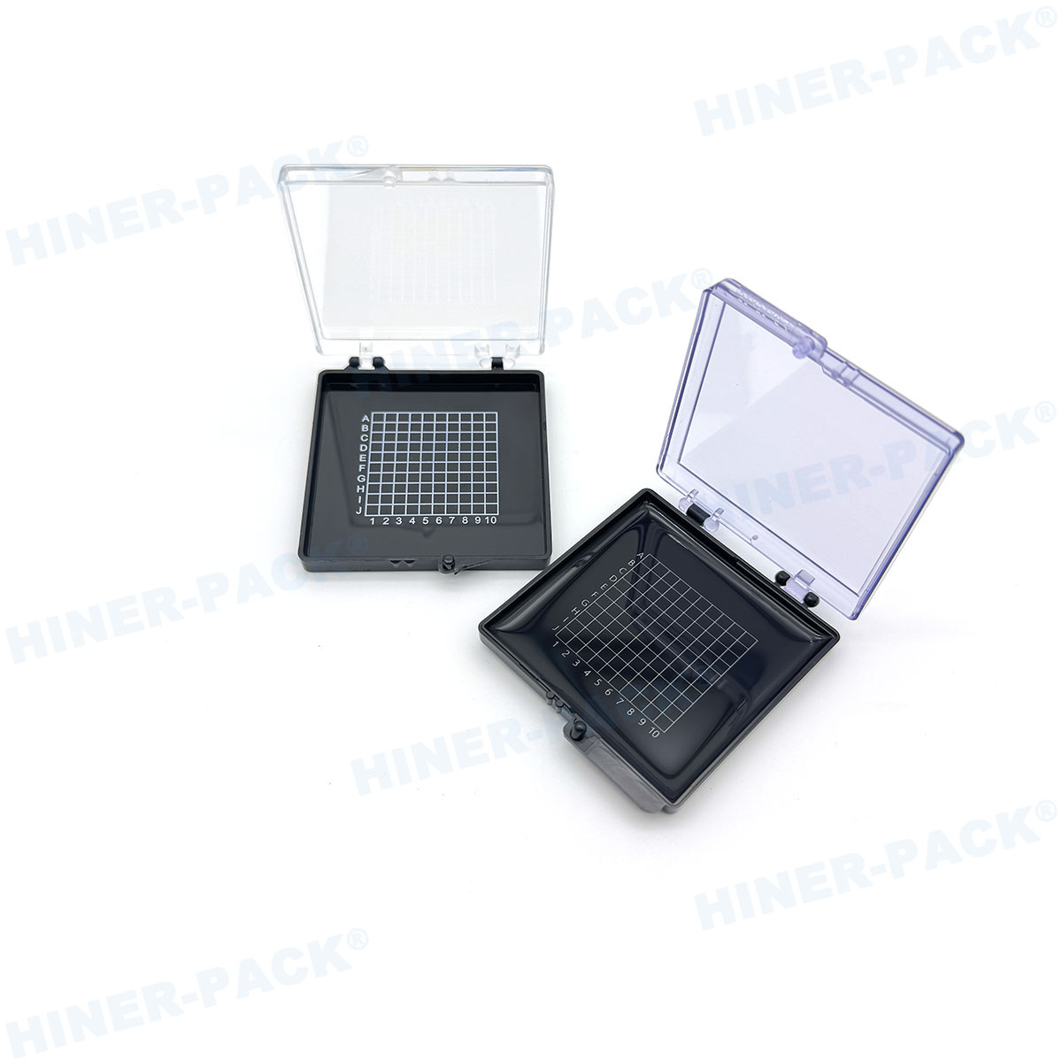
The JEDEC tray standard refers to a set of guidelines established by JEDEC Solid State Technology Association. JEDEC is a global leader in developing standards for the microelectronics industry. This standard specifically defines the dimensions, materials, and design requirements for trays used in semiconductor packaging. These trays hold wafers or chips during manufacturing, testing, and shipping.
Trays compliant with the JEDEC tray standard ensure interoperability across different equipment and facilities. They prevent misalignment and physical stress on components. This reduces scrap rates and improves yield. The standard covers various tray types, including those for bare wafers and finished packages.
Key elements include pocket sizes, tray thickness, and stacking features. By following the JEDEC tray standard, companies achieve consistency. This is crucial in high-volume production environments. Hiner-pack, a trusted brand in packaging solutions, emphasizes adherence to these standards for client success.
History and Development of JEDEC Tray Standards
The JEDEC tray standard evolved alongside the semiconductor industry. In the early days, handling methods were inconsistent. This led to frequent damage and inefficiencies. JEDEC recognized the need for uniformity. In the 1990s, they began formalizing tray specifications.
Initial efforts focused on basic dimensions. Over time, the JEDEC tray standard expanded to include materials like conductive plastics. These materials prevent electrostatic discharge (ESD). ESD can ruin sensitive semiconductors. The standard also adapted to new wafer sizes, such as 300mm.
Today, the JEDEC tray standard is regularly updated. This ensures compatibility with advancing technologies. Hiner-pack actively participates in these updates. Their expertise helps shape practical implementations. The history shows a commitment to industry-wide collaboration and innovation.
Key Specifications and Dimensions in JEDEC Tray Standard
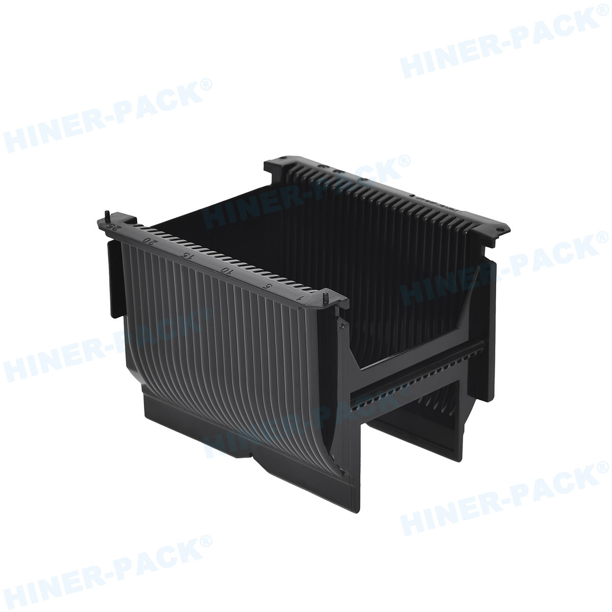
Understanding the technical details of the JEDEC tray standard is vital for compliance. The standard specifies precise measurements. For example, trays for 300mm wafers have defined outer dimensions. Typical sizes are 336mm x 336mm or similar. Pocket depths and spacings are also standardized.
Materials must meet rigidity and ESD requirements. Commonly used materials include carbon-loaded polycarbonate. This provides durability and static protection. The JEDEC tray standard also defines stacking features. These allow secure stacking during storage and transit.
Weight limits and tolerance levels are included. This ensures trays fit automated handling systems. Hiner-pack designs trays with these specs in mind. Their products undergo rigorous testing. This guarantees they meet the JEDEC tray standard exactly. Such precision reduces downtime and errors.
Applications in the Semiconductor Industry
The JEDEC tray standard is widely used across semiconductor processes. From fabrication to assembly, trays play a key role. In wafer fabrication, trays protect bare wafers. They move wafers between etching, doping, and polishing steps.
During testing, trays hold chips for electrical validation. Automated test equipment relies on standardized trays. This speeds up throughput. In packaging, trays transport finished ICs to molding and marking stations. The JEDEC tray standard ensures smooth transitions.
Shipping and logistics also benefit. Standardized trays fit into common shipping containers. This optimizes space and security. Hiner-pack supplies trays for all these stages. Their solutions align with the JEDEC tray standard. This supports clients in achieving efficient workflows.
Benefits of Adopting JEDEC Tray Standard
Implementing the JEDEC tray standard offers numerous advantages. First, it reduces component damage. Uniform trays minimize mishandling. This lowers scrap rates and saves money. Second, it enhances compatibility. Equipment from different vendors works seamlessly with standardized trays.
Third, the JEDEC tray standard improves scalability. Companies can expand operations without retooling. Fourth, it supports automation. Robots and conveyors depend on consistent tray designs. This boosts production speed. Fifth, it aids in quality control. Standardized trays simplify inspection processes.
Hiner-pack highlights these benefits for clients. Their trays comply fully with the JEDEC tray standard. This ensures reliability and cost-effectiveness. In a competitive market, such standards are a strategic advantage. They foster innovation and growth.
Hiner-pack's Implementation of JEDEC Tray Standard
Hiner-pack is a leading provider of semiconductor packaging solutions. They integrate the JEDEC tray standard into all their tray products. Their design team follows JEDEC guidelines meticulously. This results in trays that excel in performance.
Hiner-pack uses advanced materials. These meet ESD and durability requirements. Their manufacturing process includes quality checks. Each tray is verified against the JEDEC tray standard. This guarantees precision. Clients report fewer defects and higher efficiency.
The company also offers customization within standard limits. For instance, they can tweak colors or labeling. But core dimensions always adhere to the JEDEC tray standard. Hiner-pack's commitment ensures they remain a trusted partner. Their trays support diverse applications, from memory chips to processors.
Future Trends and the JEDEC Tray Standard
The semiconductor industry continues to evolve. Trends like smaller nodes and 3D packaging pose new challenges. The JEDEC tray standard must adapt to these changes. JEDEC committees are already working on updates. These may include trays for thinner wafers or new materials.
Sustainability is another focus. Future standards might emphasize recyclable materials. Hiner-pack is proactive in this area. They research eco-friendly options while maintaining compliance. The JEDEC tray standard will likely incorporate such innovations.
Automation and IoT will drive demand for robust trays. The JEDEC tray standard will ensure these systems interoperate globally. Hiner-pack plans to lead in these developments. Their ongoing investment in R&D aligns with JEDEC's vision. This future-proofs their products and services.
The JEDEC tray standard is a cornerstone of modern semiconductor manufacturing. It provides the consistency needed for high-yield, low-cost production. From history to specifications, this standard impacts every stage of the supply chain. Companies that adopt it gain a competitive edge.
Hiner-pack exemplifies how to leverage the JEDEC tray standard effectively. Their trays meet rigorous requirements while supporting innovation. As technology advances, this standard will continue to play a vital role. Embracing the JEDEC tray standard is not just about compliance—it's about driving excellence in the electronics world.
Frequently Asked Questions (FAQs)
Q1: What is the primary purpose of the JEDEC tray standard?
A1: The primary purpose of the JEDEC tray standard is to establish uniform dimensions, materials, and design specifications for trays used in semiconductor handling. This ensures compatibility across different manufacturing and testing equipment, reduces component damage, and improves operational efficiency in the electronics industry.
Q2: How does the JEDEC tray standard benefit small semiconductor businesses?
A2: The JEDEC tray standard benefits small businesses by lowering entry barriers. It provides a proven framework for packaging, reducing the need for custom solutions. This minimizes costs, enhances reliability, and allows smaller firms to integrate easily into global supply chains, often with support from suppliers like Hiner-pack.
Q3: Are Hiner-pack trays fully compliant with the JEDEC tray standard?
A3: Yes, Hiner-pack trays are fully compliant with the JEDEC tray standard. They are designed and manufactured to meet all specified dimensions, material requirements, and performance criteria. Hiner-pack conducts rigorous testing to ensure adherence, making their trays a reliable choice for semiconductor applications.
Q4: Can the JEDEC tray standard be used for non-semiconductor components?
A4: While the JEDEC tray standard is tailored for semiconductors, its principles can sometimes apply to other delicate components, such as in optoelectronics or MEMS devices. However, for optimal results, it's best to use it as intended or consult standards for specific industries to avoid compatibility issues.
Q5: How often is the JEDEC tray standard updated, and how can companies stay informed?
A5: The JEDEC tray standard is updated periodically to reflect technological advancements, typically every few years. Companies can stay informed by subscribing to JEDEC publications, participating in industry forums, or partnering with suppliers like Hiner-pack, who monitor changes and update their products accordingly.