In semiconductor backend operations—from wafer sort to final assembly and
test—the handling and shipping of singulated integrated circuits demand
packaging that meets stringent industry specifications. IPC
compliant trays represent the benchmark for reliability, ensuring
that components remain free from electrostatic discharge (ESD) damage, physical
contamination, and mechanical stress throughout the supply chain. The IPC/JEDEC
J-STD-033 and IPC-1601 standards define critical parameters: material
resistivity, dimensional tolerances, outgassing limits, and cleanliness levels.
Deviations in any of these areas can lead to latent failures, yield loss, or
field returns. This article provides a technical examination of the material
science, manufacturing controls, and quality assurance protocols that
distinguish high-grade semiconductor trays from commoditized alternatives,
drawing on field data from Hiner-pack implementations
across OSAT (outsourced semiconductor assembly and test) facilities and IDM
(integrated device manufacturer) assembly lines.
1. Material Selection: Balancing ESD Protection with Mechanical
Performance
The foundation of any IPC
compliant tray is its polymer formulation. Base resins must be
modified to achieve specific surface and volume resistivity while maintaining
structural rigidity across temperature ranges encountered during baking, reflow,
and storage.
1.1 Static Dissipative vs. Conductive Properties
IPC-1601 defines three categories for ESD control in handling trays:
Conductive (10² to 10⁵ Ω/sq): Typically achieved with
carbon fiber or carbon powder loading. Used for high-risk environments where
rapid charge dissipation is mandatory.
Static Dissipative (10⁵ to 10¹¹ Ω/sq): Achieved with
carbon-loaded polycarbonate (PC), polyethylene terephthalate (PET), or
polyphenylene sulfide (PPS). This range provides controlled charge decay without
the triboelectric charging risks associated with insulative materials.
Antistatic (10¹¹ to 10¹² Ω/sq): Surface resistivity
modified via topical coatings or internal antistatic agents. Suitable for less
sensitive components but requires regular cleaning to maintain
efficacy.
For advanced nodes (≤28 nm) and sensitive RF or memory devices, conductive or
dissipative trays are mandatory. Surface resistivity measurements are performed
per ANSI/ESD STM11.11 and must be revalidated periodically as additives can
migrate or degrade over time.
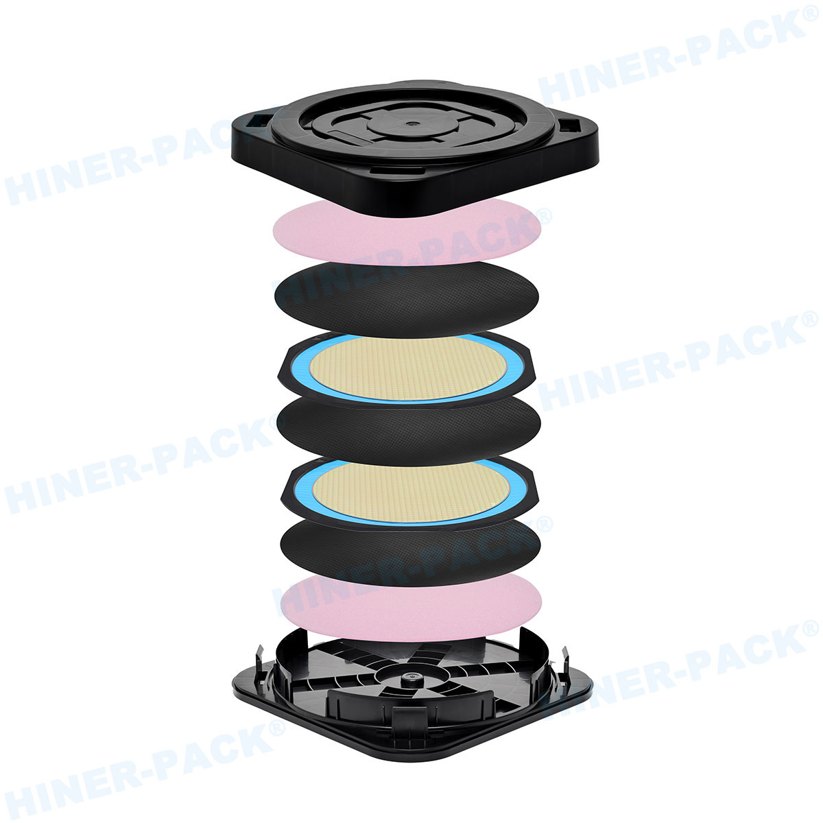
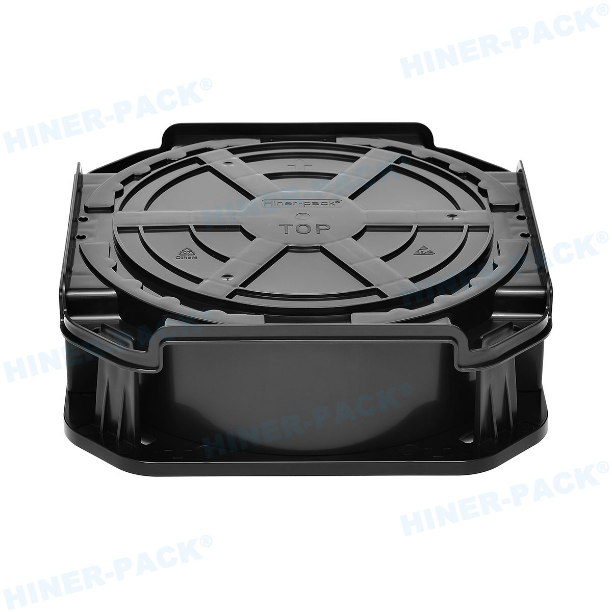
2. Dimensional Specifications: Pocket Geometry and Coplanarity Control
Semiconductor trays are not merely containers; they are precision fixtures
that must align with automated handling equipment—pick-and-place machines, test
handlers, and vision inspection systems. Dimensional deviations cause jams,
mis-picks, and component damage.
2.1 JEDEC and EIAJ Standards
Tray dimensions follow JEDEC (Joint Electron Device Engineering Council) and
EIAJ (Electronic Industries Association of Japan) standards. Key parameters
include:
Pocket depth and width: Tolerances typically ±0.05 mm to
ensure consistent component orientation without excessive play.
Pocket-to-pocket pitch: Cumulative error across the tray
matrix must not exceed ±0.1 mm to maintain alignment with vacuum nozzle
arrays.
Overall tray flatness: Warpage limited to ≤0.5 mm across
the tray diagonal to prevent vacuum pickup failures.
Mold flow analysis during tooling design is employed to minimize sink marks
and residual stresses that could lead to warpage after temperature cycling.
Hiner-pack utilizes precision injection molding with in-line
optical measurement to verify pocket dimensions on every production batch.
3. Cleanliness and Contamination Control
Contamination from packaging materials—ionic residues, particulates, or
outgassed volatiles—can cause corrosion, wire bond failures, or die attach
delamination. IPC-1601 and J-STD-033 prescribe limits for packaging
materials.
3.1 Ionic Cleanliness and Particulate Limits
High-performance trays undergo rigorous cleaning and testing:
Ionic contamination: Measured per IPC-TM-650, Method
2.3.28. Acceptable limits: ≤0.5 µg/cm² NaCl equivalents for critical
devices.
Particle count: Liquid particle counters (LPC) test per
IEST-RP-CC012. Tray surfaces must meet Class 1000 (ISO 6) cleanliness for
devices with sub-100 µm bond pad spacing.
Outgassing: Per NASA/ESA specifications (ASTM E595), trays
must exhibit total mass loss (TML) ≤1.0% and collected volatile condensable
materials (CVCM) ≤0.1% to avoid fogging of optical surfaces or contamination of
hermetic packages.
Manufacturing processes for IPC
compliant trays include ultrasonic cleaning, deionized water
rinsing, and controlled drying in Class 1000 cleanroom environments. Packaging
is performed in ESD-safe, heat-sealed bags with desiccant and humidity indicator
cards when specified.
4. Thermal Performance: Bake Cycles and High-Temperature Processing
Semiconductor devices are frequently subjected to pre-conditioning bake
cycles (125°C for 24 hours) and lead-free reflow profiles (peak 260°C). Trays
must maintain dimensional stability and not release contaminants under these
conditions.
4.1 Material Heat Deflection and Continuous Use Temperature
Key thermal properties:
Heat deflection temperature (HDT) at 1.82 MPa: For
polycarbonate (PC) trays, HDT is typically 125–130°C; for polyetheretherketone
(PEEK) or polyphenylene sulfide (PPS), HDT exceeds 200°C.
Continuous use temperature: PC trays are rated for
100–120°C; high-temperature grades (PPS, PEI) withstand 180–220°C continuous
exposure.
Thermal expansion coefficient (CTE): Must match device
package CTE to minimize stress. Typical tray CTE ranges from 40–80 ppm/°C;
package CTE is 15–25 ppm/°C for molded compounds, requiring careful tray
material selection to avoid excessive pocket deformation.
For trays used in lead-free reflow processes, materials must be rated for
260°C peak temperatures. Standard PC trays are not suitable; only
high-temperature thermoplastics (PPS, PEI, or PEEK) are acceptable.
5. Compatibility with Automated Handling Equipment
Modern semiconductor assembly lines utilize high-speed automation. Trays must
interface reliably with:
JEDEC tray stackers/destackers: Tray corner designs, rib
patterns, and stack height tolerances must match equipment specifications to
prevent misfeeds.
Pick-and-place systems: Pocket geometry must allow vacuum
nozzle access without interference; chamfered pocket edges facilitate component
centering.
Vision inspection systems: Tray color and surface finish
must provide sufficient contrast for lead and body recognition. Matte black or
dark gray dissipative materials are standard to minimize reflections.
Incompatibility often manifests as throughput reduction or jam rates
exceeding 0.5%. Hiner-pack provides dimensional data packages
to customers for integration validation prior to volume procurement.
6. Quality Assurance and Traceability
Semiconductor manufacturers demand full traceability and documented
conformance to IPC and JEDEC standards. A robust quality program includes:
6.1 Incoming Material Certifications
Each batch of raw resin must be accompanied by certificates of analysis (CoA)
confirming:
Surface and volume resistivity per ANSI/ESD STM11.12.
Melt flow index (MFI) to ensure consistent moldability.
Moisture content (≤0.02% for hygroscopic materials) to prevent hydrolytic
degradation.
6.2 In-Process and Final Inspection
Production controls include:
First-article inspection (FAI) per AS9102, measuring critical dimensions
across all pockets.
100% vision inspection for flash, voids, or contaminant inclusions.
Sampled dimensional verification using coordinate measurement machines (CMM)
at defined intervals.
Resistivity testing per batch using concentric ring probes.
6.3 Lot Traceability
Each tray is marked with mold cavity number, date code, and batch ID. This
enables root cause analysis in the event of field issues and supports
semiconductor industry requirements for full supply chain transparency.
7. Lifecycle Considerations: Reusability, Cleaning, and End-of-Life
Many semiconductor trays are designed for multiple use cycles. Key factors
influencing reusable tray economics:
Mechanical durability: Trays must withstand 500+ handling
cycles without cracking, warping, or pocket deformation. High-impact grades of
polycarbonate or polypropylene are preferred.
Cleanability: Tray materials must resist common cleaning
agents (isopropyl alcohol, deionized water, mild detergents) without surface
degradation or resistivity shift.
Recyclability: Single-polymer construction (e.g., 100%
polycarbonate) facilitates closed-loop recycling, reducing environmental
footprint and material costs for high-volume users.
Suppliers offering tray washing and recertification services help customers
maximize asset utilization while maintaining cleanliness specifications.
Frequently Asked Questions (FAQ)
Q1: What is the difference between IPC compliant trays and standard shipping
trays?
A1: Standard trays may not undergo the rigorous material
testing, dimensional verification, and cleanliness controls required by IPC-1601
and J-STD-033. IPC compliant trays are manufactured from
certified static-dissipative or conductive materials with documented
resistivity, ionic cleanliness, and outgassing profiles. They also adhere to
precise JEDEC/EIAJ pocket geometries essential for automated handling. Using
non-compliant trays risks ESD damage, contamination-induced bond failures, and
equipment jams—all of which can result in yield loss exceeding 2–3% in
high-volume assembly lines.
Q2: How do I verify that a tray is truly IPC compliant?
A2: Request a compliance package from the supplier that
includes: material resistivity test reports (ANSI/ESD STM11.11), dimensional
certification (first article inspection report per AS9102), ionic cleanliness
test results (IPC-TM-650), and outgassing data (ASTM E595). For critical
applications, conduct incoming inspection on a representative sample using your
own metrology and ESD measurement equipment. Suppliers like
Hiner-pack provide full traceability documentation with each
shipment, including lot-specific CoAs.
Q3: Can IPC compliant trays withstand lead-free reflow temperatures
(260°C)?
A3: Standard polycarbonate or PET trays cannot withstand
260°C; they will deform and release volatile contaminants. For lead-free reflow
processing, trays must be manufactured from high-temperature thermoplastics such
as polyphenylene sulfide (PPS), polyetherimide (PEI), or polyetheretherketone
(PEEK). These materials maintain dimensional stability up to 260°C and have low
outgassing characteristics. Always verify the continuous use temperature rating
with the supplier before using trays in reflow ovens.
Q4: What is the typical shelf life and storage condition for IPC compliant
trays?
A4: Trays should be stored in their original ESD-safe,
heat-sealed packaging until use. Recommended storage conditions: temperature
20–25°C, relative humidity 30–60%. Shelf life is typically 24 months from date
of manufacture when stored properly. Prolonged exposure to UV light, elevated
humidity, or aggressive chemicals can degrade ESD properties. For hygroscopic
materials like polycarbonate, trays should be baked at 80–100°C for 4–8 hours
before use if the moisture barrier packaging has been compromised.
Q5: How do I select the correct tray pocket size for a given semiconductor
package?
A5: Pocket dimensions are specified by the package type
(e.g., QFP, BGA, SON) and body size. Refer to JEDEC standards for standard
package outlines (JEDEC MO series). The pocket must allow a clearance of 0.2–0.5
mm around the package body to accommodate variations while preventing excessive
movement. Pocket depth should be 0.3–0.8 mm greater than package thickness to
allow vacuum nozzle access. For custom or emerging package formats, request a
sample tray and conduct pick-and-place trials to validate fit and handling
reliability before committing to volume orders.
Selecting and validating IPC
compliant trays is a critical step in semiconductor supply chain
risk management. From material resistivity to pocket geometry, each
specification directly impacts assembly yields, device reliability, and
automation efficiency. Hiner-pack combines engineering
expertise with rigorous quality systems to deliver trays that meet the most
demanding requirements of OSATs, IDMs, and EMS providers worldwide.


