In advanced semiconductor manufacturing—from front-end fabs to backend
assembly—the protection of wafers from particulate contamination, moisture, and
physical damage during transport is non-negotiable. Among the most critical
tools in this logistics chain are vacuum wafer carriers. These specialized enclosures
create a controlled, often inert, microenvironment that isolates delicate
substrates from atmospheric fluctuations and mechanical stresses. For process
engineers and fab managers, the selection and qualification of such carriers
directly influence yield, especially as device nodes shrink and wafer diameters
increase.
This article examines the engineering principles, material science, and
automation requirements defining modern vacuum wafer carriers.
We will explore sealing mechanisms, cleanliness protocols, compatibility with
automated material handling systems (AMHS), and the growing demand for carriers
that support both 300mm fabs and advanced packaging workflows. Companies like
Hiner-pack have operationalized these
specifications, delivering carriers that bridge stringent fab requirements with
operational efficiency.
1. Core Functional Requirements of Vacuum Wafer Carriers
Unlike standard shipping trays or open FOUPs (front opening unified pods),
vacuum wafer carriers are engineered to maintain a sealed
environment, often under negative pressure or with inert gas purging. Their
primary roles include protecting wafers from oxidation, moisture absorption, and
airborne molecular contamination (AMC) during inter-fab transport, long-term
storage, or process steps requiring strict environmental control.
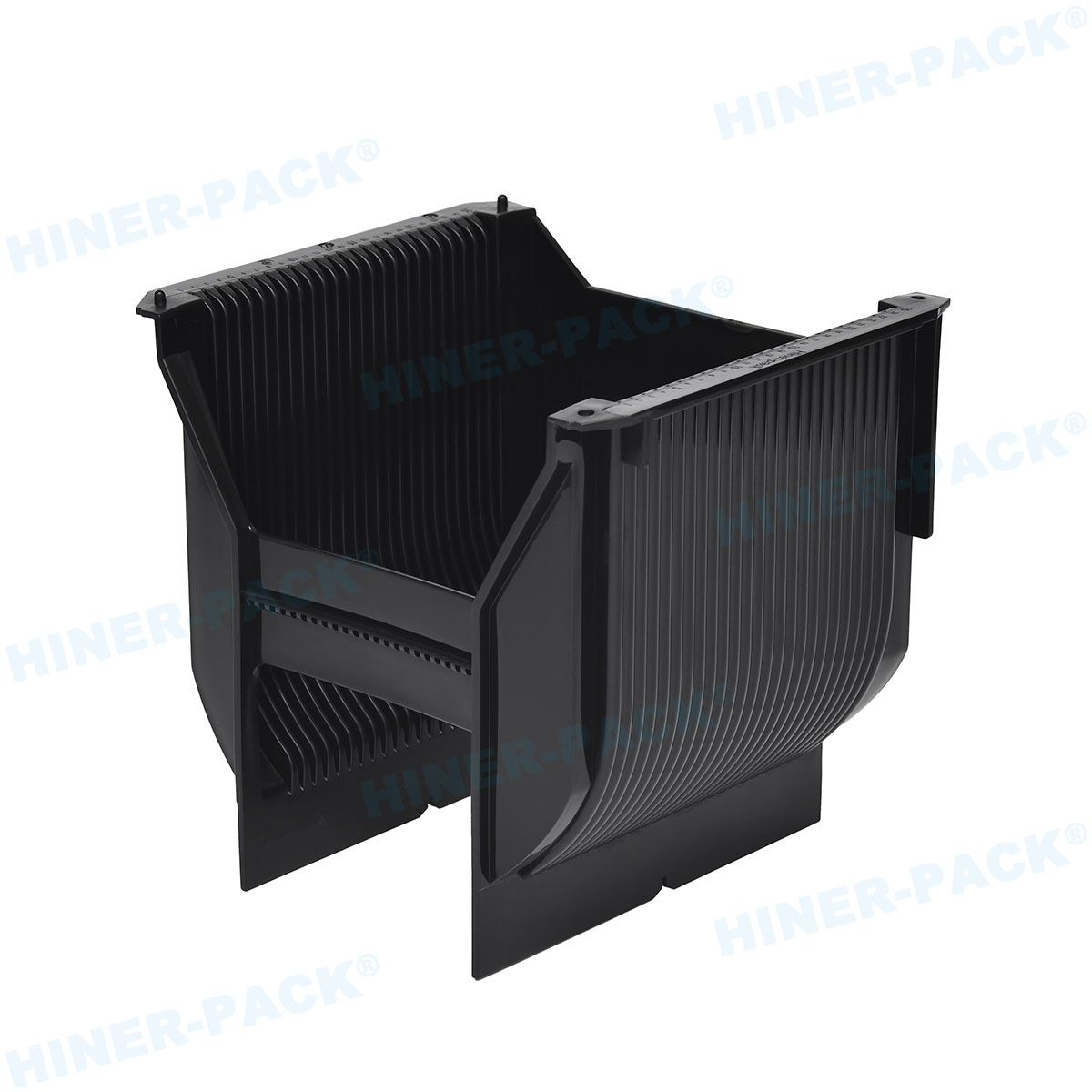
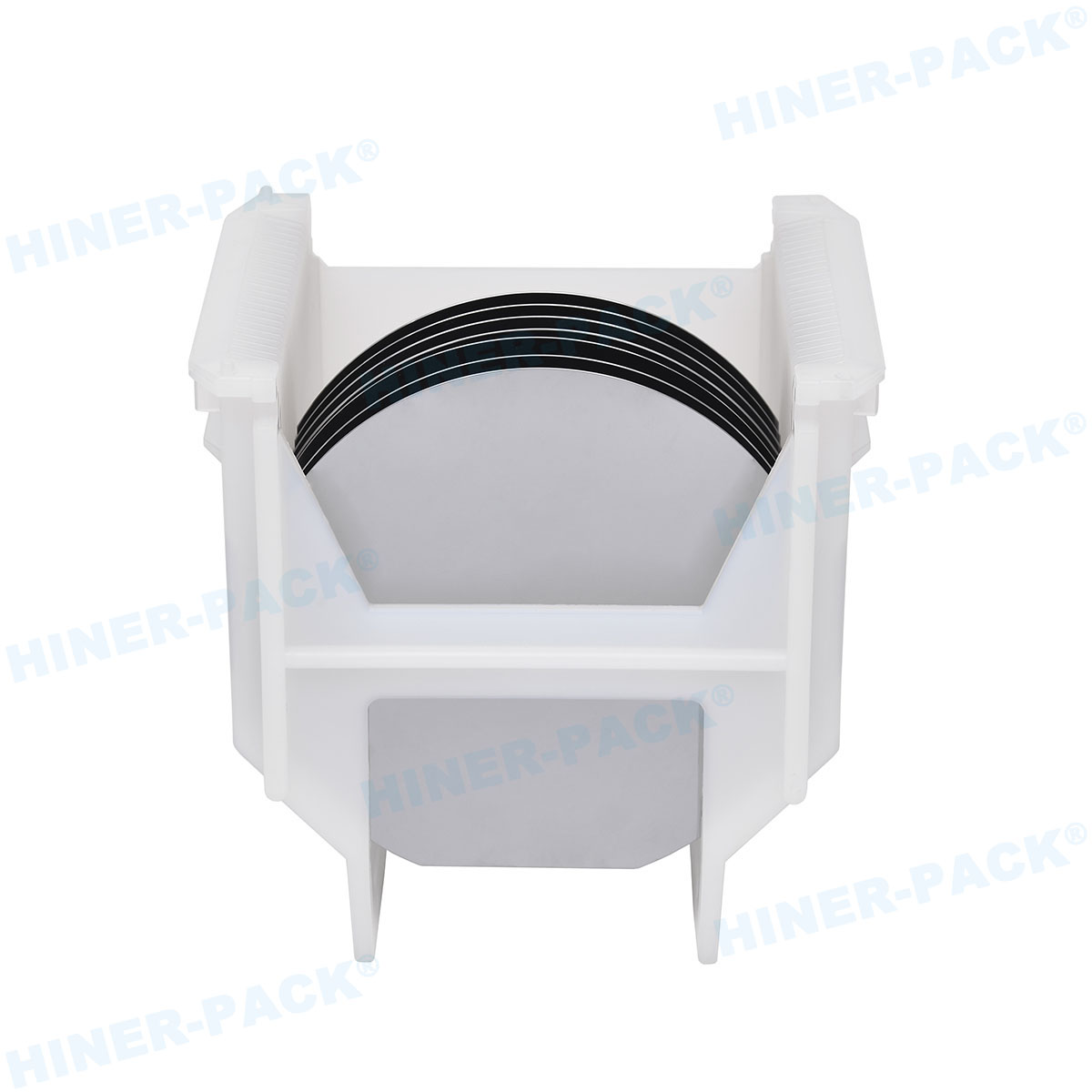
1.1 Sealing Integrity and Leak Rate Specifications
The cornerstone of any vacuum carrier is its ability to maintain a specified
vacuum level or inert atmosphere over a defined duration. Typical specifications
require leak rates below 1×10⁻⁶ atm·cc/sec for helium leakage testing, per SEMI
E72 (standard for vacuum wafer shipping containers). The sealing mechanism often
involves dual-lip elastomeric seals (fluorocarbon or perfluoroelastomer) that
resist outgassing and maintain flexibility across temperature cycles (−40°C to
125°C). Carrier bodies are commonly machined from 6061-T6 aluminum or
injection-molded carbon-fiber reinforced polycarbonate, each offering distinct
trade-offs between weight, durability, and particle generation.
For 300mm wafer applications, the carrier must also accommodate vacuum ports
with self-sealing valves that prevent contamination ingress during connection
and disconnection. These valves are qualified for thousands of mating cycles
without degrading seal performance—a critical factor in high-volume
manufacturing environments.
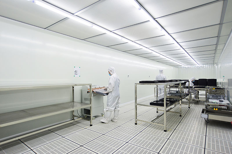
1.2 Particle Control and Cleanliness Standards
Contamination control is arguably the most stringent requirement.
Vacuum wafer carriers intended for use in cleanrooms must meet
ISO 14644-1 Class 1 or Class 2 particle specifications. This means that after
cleaning and assembly, the internal surfaces must generate fewer than 10
particles ≥0.1 µm per square centimeter when subjected to standardized airflow
or vibration tests. Materials are selected for low outgassing per ASTM E595 and
low ionic extractables per SEMI C3.2.
Leading manufacturers employ ultrasonic cleaning in deionized water followed
by vacuum baking to remove residual moisture and volatiles. The final packaging
is done in ISO Class 4 environments, often with double-bagging and nitrogen
purging to preserve cleanliness until the point of use.
2. Material Science and Structural Design for Vacuum Applications
The choice of materials in vacuum wafer carriers directly
impacts performance across three axes: structural rigidity under external
pressure, chemical compatibility with fab solvents, and electrostatic discharge
(ESD) control. Aluminum carriers offer superior thermal conductivity and
mechanical stability, making them suitable for applications requiring repeated
bake-out cycles. However, they are heavier and may require careful surface
anodization to prevent particle shedding.
Polymer-based carriers, typically using PEEK (polyetheretherketone) or
high-purity polycarbonate, provide weight reduction and inherent static
dissipation when properly compounded. For 300mm FOUP-like vacuum carriers, the
industry has gravitated toward hybrid designs: a polycarbonate shell for weight
and cost efficiency, with metal reinforcement at latch points and sealing
flanges to ensure consistent compression of the O-ring.
2.1 Thermal and Mechanical Stress Tolerance
Vacuum carriers are often subjected to thermal cycling during shipping (e.g.,
air freight at high altitude) or process holds (e.g., pre-furnace storage).
Standards such as SEMI E47 (thermal cycling test for shipping containers)
require that carriers withstand 10 cycles from −20°C to 60°C without dimensional
change exceeding 0.1 mm. For polymer carriers, this demands the use of materials
with low coefficient of thermal expansion (CTE) and adequate glass transition
temperature (Tg) above 130°C.
Mechanical shock and vibration testing per ISTA 3A or SEMI E62 ensure that
carriers protect wafers from damage during handling and transport. A
well-designed carrier decouples external forces through compliant wafer supports
(edge-contact only) and shock-absorbing base plates.
3. Automation Integration and Industry 4.0 Readiness
Modern semiconductor facilities rely on fully automated material handling
systems (AMHS). Vacuum wafer carriers must therefore
incorporate features for robotic identification, handling, and data tracking.
This includes RFID tags compliant with SEMI E142 (specification for
identification of shipping trays and carriers), machine-readable data matrix
codes, and standardized kinematic coupling interfaces for load ports.
The carrier’s base plate geometry must conform to SEMI E15.1 (specification
for tool load port) to ensure compatibility with overhead hoist transport (OHT)
vehicles and stockers. Key dimensions such as the carrier’s overall height,
latch positions, and gripper engagement points are standardized to allow
seamless transfer between equipment from different OEMs. When these
specifications are followed, changeover times between different product types
can be reduced by up to 40%, a critical metric in high-mix fabs.
4. Industry Pain Points and Engineering Solutions
Despite mature specifications, semiconductor fabs continue to face recurring
challenges with vacuum wafer carriers. These pain points often
stem from deviations in manufacturing consistency or improper handling
procedures. A data-driven examination reveals three primary areas of
concern.
Pain Point 1: Seal Degradation Leading to Vacuum Loss
In
high-volume shipping lanes, elastomeric seals can experience compression set,
micro-cracking from ozone exposure, or contamination from process residues. A
loss of vacuum integrity can result in wafer corrosion or delamination in
subsequent thermal steps. Solution: Implementing seal material with proven
resistance to fab chemicals (e.g., perfluoroelastomers like FFKM) and
establishing a seal replacement schedule based on cycle count rather than time
alone. Suppliers like Hiner-pack provide lifecycle management data for
their carriers to optimize preventive maintenance.
Pain Point 2: Particle Generation from Internal
Surfaces
After repeated cleaning cycles, anodized aluminum surfaces
may develop micro-fractures that release particles. Similarly, polymer carriers
can experience wear at wafer contact points. Solution: Using advanced coatings
such as plasma electrolytic oxidation (PEO) for aluminum, or incorporating
ultra-high molecular weight polyethylene (UHMW) inserts at wafer contact zones.
In-process particle monitoring using liquid particle counters (LPC) during
carrier requalification is essential.
Pain Point 3: Incompatibility with Automated Stocker
Systems
Carriers with slight dimensional deviations—even 0.5 mm—can
cause jamming in high-density stockers, leading to downtime. Solution:
Implementing 100% dimensional inspection using coordinate measuring machines
(CMM) and ensuring that carrier suppliers provide SPC data for critical
dimensions. Certifications such as ISO 9001:2015 with specific focus on
precision molding or machining are mandatory.
5. Advanced Applications: Vacuum Carriers for 3D Integration and Thin
Wafers
The rise of 3D integration, fan-out wafer-level packaging (FOWLP), and thin
wafer processing (below 100 µm) has introduced new requirements for
vacuum wafer carriers. Thin wafers are extremely fragile and
sensitive to edge stress; traditional carriers with rigid pockets can induce
micro-cracking during vacuum sealing. New designs incorporate soft-contact wafer
retainers, such as PEEK or silicone edge-grippers, that distribute clamping
force evenly.
Additionally, carriers used in temporary bonding/debonding processes must
withstand temperatures up to 250°C and chemical exposure to solvents like NMP
(N-methyl-2-pyrrolidone). For these applications, all-metal carriers (stainless
steel or aluminum with PEO coating) are preferred, equipped with
high-temperature seals and vacuum gauges for real-time monitoring. The
convergence of vacuum wafer carriers with sensor
technology—embedded pressure transducers and RFID-logged environmental data—is
becoming a differentiator for high-reliability supply chains.
6. Qualification and Compliance: Meeting Global Semiconductor
Specifications
Qualifying a vacuum wafer carrier for production use requires exhaustive
documentation and testing. Fab procurement teams typically demand the following
evidence:
Leak test reports per SEMI E72, including helium mass spectrometry data for
each carrier.
Cleanliness verification: particle counts (≥0.1 µm and ≥0.3 µm) per SEMI
C3.2, plus ion chromatography results for fluoride, chloride, sulfate, and other
extractables.
Outgassing analysis per ASTM E595 or SEMI E108, with total mass loss (TML)
< 0.1% and collected volatile condensable materials (CVCM) < 0.01%.
ESD testing per ANSI/ESD STM11.11 to confirm surface resistivity in the
static-dissipative range (1E5 to 1E12 ohms/sq).
Dimensional verification reports for key features: flange flatness, latch
position, kinematic coupling alignment, and wafer pocket geometry.
Reputable suppliers, including vacuum wafer carriers specialists, provide this
documentation as part of their standard shipment to reduce customer
qualification lead times.
7. Future Directions: Sustainability, Sensor Integration, and
Standardization
As the semiconductor industry pushes toward net-zero goals, vacuum
wafer carriers face scrutiny regarding their lifecycle environmental
impact. Reusable carriers made from recyclable polymers or aluminum are
increasingly favored over single-use options, provided they can be requalified
after cleaning. New standards under development within SEMI focus on defining
maximum cleaning cycles and criteria for requalification, balancing
sustainability with contamination risk.
Simultaneously, the adoption of Industry 4.0 principles is driving the
integration of IoT-enabled carriers. These “smart” carriers incorporate sensors
that log temperature, humidity, vacuum level, and shock events during transit,
transmitting data to cloud-based MES systems. Such capabilities allow for
predictive maintenance and real-time anomaly detection, reducing the risk of
undetected environmental excursions that could compromise wafer integrity.
The role of vacuum wafer carriers in semiconductor
manufacturing extends far beyond simple transportation. They are
precision-engineered systems that maintain the purity and integrity of wafers
across the most critical stages of production. From advanced 3nm logic to
heterogeneous integration, the selection of a vacuum carrier involves careful
consideration of sealing technology, material cleanliness, automation
compatibility, and lifecycle management. As fabs become increasingly automated
and process windows narrow, the collaboration between device makers and carrier
specialists becomes essential. Companies like Hiner-pack exemplify how deep expertise in materials
science and metrology translates industry standards into reliable,
high-performance logistics solutions. The future will see even tighter
integration of digital intelligence with carrier hardware, ensuring that the
protective envelope around each wafer is as sophisticated as the devices
themselves.
Frequently Asked Questions (FAQ)
Q1: What is the difference between a vacuum wafer carrier and a
standard FOUP?
A1: A FOUP (front opening unified
pod) is designed primarily for 300mm wafer transport within a fab, using a door
that seals against the pod shell but typically does not maintain a sustained
vacuum or inert gas purge. In contrast, a vacuum wafer carrier is engineered to hold a vacuum or controlled atmosphere (e.g., nitrogen) for
extended periods—often days or weeks—and includes valves and seals that allow
evacuation and backfilling. Vacuum carriers are used for inter-fab shipping,
long-term storage, and processes requiring a defined low-moisture or low-oxygen
environment.
Q2: How are vacuum wafer carriers cleaned and requalified for
reuse?
A2: Cleaning typically follows a validated
process: pre-rinse with deionized water, ultrasonic cleaning in a surfactant
solution, multiple DI water rinses, and final drying in a Class 10 cleanroom
environment. After cleaning, carriers undergo requalification tests including
particle count verification (using liquid particle extraction), leak testing per
SEMI E72, and surface resistivity checks. A maximum number of cleaning cycles is
established based on material wear and seal degradation studies.
Q3: Can vacuum wafer carriers be used for thin wafers (under 100 µm)
without causing damage?
A3: Yes, but they require
specialized wafer retention designs. Traditional carriers with rigid pockets can
cause edge chipping or stress fractures on thin wafers during vacuum sealing.
Advanced carriers incorporate soft-contact materials like PEEK, silicone, or
UHMW at contact points, and often use edge-gripping rather than full-pocket
support. Additionally, the vacuum level may be modulated to prevent excessive
force on the wafer. Always verify carrier compatibility with the wafer thickness
and bow specifications.
Q4: What materials are commonly used for high-temperature vacuum
wafer carriers (above 200°C)?
A4: For applications
exceeding 200°C, such as post-bond annealing or metal sintering, standard
polycarbonate carriers are unsuitable. All-metal carriers made from 6061
aluminum with plasma electrolytic oxidation (PEO) coating or stainless steel are
used. For polymer-based high-temperature carriers, PEEK (polyetheretherketone)
or Torlon (polyamide-imide) are preferred due to their high glass transition
temperatures (Tg > 250°C) and low outgassing. Seals must be upgraded to
perfluoroelastomers (FFKM) rated for continuous operation at 260°C.
Q5: How do I ensure that a vacuum wafer carrier is compatible with my
fab’s automated handling system?
A5: Compatibility
is determined by three factors: kinematic coupling design (must match SEMI E15.1
and the specific load port type), RFID tag placement and protocol (per SEMI
E142), and overall carrier dimensions (height, width, depth) as defined by the
AMHS supplier. Request a dimensional compliance report from the carrier
manufacturer that maps their design to your fab’s equipment interface
specifications. Many suppliers, including vacuum wafer carriers providers, offer
pre-qualification services to test carriers on your AMHS before full
deployment.