
In the relentless pursuit of smaller geometries and higher yields, the semiconductor industry has pushed process tolerances to atomic scales. At these dimensions, the environment surrounding a wafer during storage and transport is no longer just a logistical detail—it is an extension of the cleanroom itself. Moisture barrier wafer carriers have emerged as a critical tool to combat the "hidden killer" in fabs: adsorbed water vapor and its devastating effects on nano-scale features. This article provides a technical deep-dive into the science, materials, and selection criteria for these specialized carriers, referencing industry best practices and solutions from leading suppliers like Hiner-pack.
The Science of Moisture Control in Wafer Handling
How Moisture Affects Wafer Integrity and Yield
Water molecules, with their small size and polar nature, are incredibly pervasive. In semiconductor manufacturing, moisture can lead to several failure mechanisms:
Hygroscopic Swelling: Photoresists and low-k dielectric materials absorb moisture, causing dimensional changes that destroy overlay accuracy in multi-patterning lithography.
Corrosion and Oxidation: Metal interconnects, particularly copper and cobalt, oxidize rapidly in the presence of humidity, increasing contact resistance and leading to open circuits.
Defect Formation: Water vapor reacts with process residues to form particles (e.g., ammonium hydroxide crystals) that scratch or contaminate the wafer surface.
Threshold Voltage Shifts: Adsorbed moisture on gate oxides alters the electrical properties of transistors, impacting device performance and reliability.
Defining Moisture Barrier Properties: WVTR and Beyond
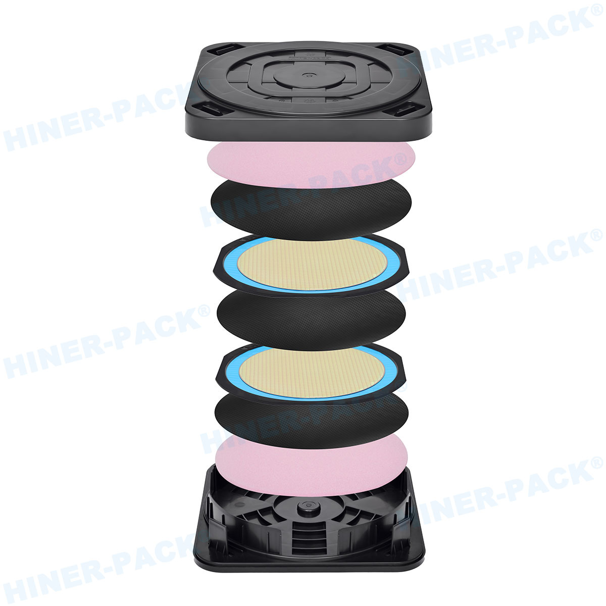
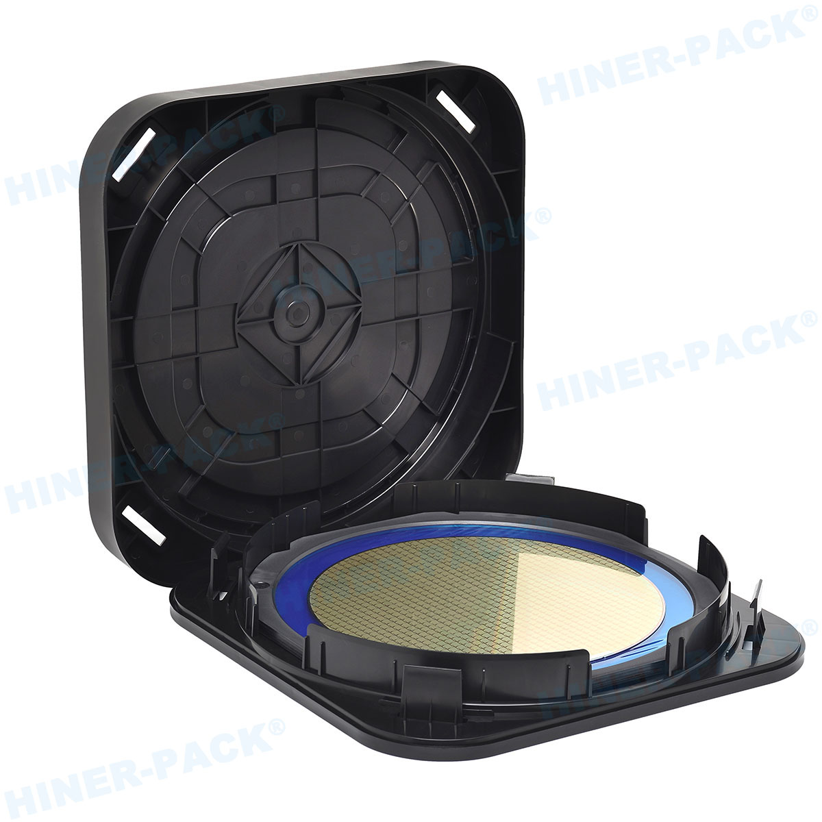
The effectiveness of a moisture barrier wafer carrier is quantified primarily by its Water Vapor Transmission Rate (WVTR). Advanced carriers achieve WVTR values below 0.01 g/m²/day, often measured using MOCON or calcium corrosion tests. However, the barrier performance is not just about the bulk material; it is equally dependent on the seal design, gasket materials, and the absence of microscopic leaks at the carrier interface. Modern carriers are engineered to maintain an internal environment of <5% relative humidity (RH) for extended periods, effectively acting as a "dry room" for individual lots.
Material Innovations Driving Moisture Barrier Performance
Advanced Polymer Blends and Nanocomposites
Traditional polycarbonate (PC) and PEEK, while mechanically robust, offer limited moisture barrier properties. Next-generation moisture barrier wafer carriers utilize multi-layer constructions or nanocomposite materials. For example, incorporating nano-clays (montmorillonite) or graphene platelets into a polymer matrix creates a tortuous path that dramatically slows water diffusion. Hiner-pack has pioneered the use of cyclic olefin copolymer (COC) blends with integrated desiccant technology, achieving near-hermetic performance while maintaining ESD safety (surface resistivity 10⁵–10⁹ Ω/sq).
The Role of Desiccants and Active Moisture Absorption
Passive barrier materials slow moisture ingress, but active moisture absorption is required to manage the moisture that is inevitably present from the loading process or outgassing from the carrier itself. Integrated desiccants—either embedded in the polymer or as replaceable cartridges—chemically or physically bind water molecules. Silica gel, molecular sieves, and calcium oxide are common, but advanced carriers use humidity-indicating desiccants that change color when saturation is approaching, allowing proactive maintenance.
Surface Engineering and Coatings
Plasma treatment or application of ultra-thin glass-like coatings (SiOx or DLC) on the interior surfaces of the carrier can further enhance the moisture barrier. These coatings also reduce particle shedding and improve cleanability, addressing another major contamination vector.
Moisture Barrier Wafer Carriers vs. Standard Carriers: A Comparative Analysis
The divergence in performance between standard FOUPs/FOSBs and dedicated moisture barrier designs is stark, particularly for sensitive processes like EUV lithography or MEMS fabrication.
WVTR: Standard carriers: > 0.5 g/m²/day | Advanced Moisture Barrier Carriers: < 0.005 g/m²/day.
Internal RH (after 7 days): Standard carriers: Equilibrium with ambient (40-60%) | Moisture Barrier Carriers: <5% (with desiccant).
Outgassing (Total Mass Loss): Standard: >0.1% | Moisture Barrier Engineered: <0.01% (ASTM E595).
Seal Technology: Standard carriers often have simple labyrinth seals; high-performance carriers feature compressible elastomeric gaskets with low permeability.
Critical Applications in Semiconductor Manufacturing
Protection of EUV and Sensitive Thin Films
Extreme Ultraviolet (EUV) lithography introduces reflective masks and photoresists that are exceptionally sensitive to moisture-induced swelling and contamination. A single water molecule can absorb EUV light, causing flare and pattern defects. Moisture barrier wafer carriers are mandatory for storing and transporting EUV blanks and patterned wafers between exposure steps. They maintain a pristine, dry environment that prevents "haze" formation on mask surfaces.
Long-Term Storage and Safe Transit in Humid Environments
For wafer banking, die banks, or shipping finished wafers to outsourced assembly and test (OSAT) facilities in tropical climates, moisture protection is non-negotiable. Carriers equipped with vacuum-seal capabilities or integrated purge ports (for nitrogen or clean dry air) ensure that wafers remain contamination-free for months. Hiner-pack offers customized shipping solutions that combine mechanical shock absorption with military-spec moisture barrier films, reducing the risk of "popcorning" during reflow soldering for packaged devices.
Integration with Automated Material Handling Systems (AMHS)
Modern fabs rely on overhead hoist transports (OHT) and stockers. Moisture barrier carriers must maintain their hermetic integrity while being compatible with standard SEMI E15.1 and E62 specifications. This requires precision molding and strict dimensional tolerances to ensure smooth handling without compromising the seal. Advanced carriers now incorporate RFID tags that log internal humidity history, providing a complete digital trace.
Addressing Industry Pain Points: Contamination, Outgassing, and ESD
Beyond moisture, the carrier itself can be a source of contamination. Amines and siloxanes outgassed from standard plastics can poison gate oxides or cause "gate oxide integrity" (GOI) failures. High-performance moisture barrier wafer carriers are manufactured from ultra-high-purity resins and undergo rigorous post-molding cleaning and surface passivation. They are often baked in vacuum ovens to drive out residual volatiles before shipment. ESD control is equally critical; carbon nanotube (CNT)-based conductive pathways are preferred over traditional carbon black fillers to minimize particle generation.
Hiner-pack’s Approach to High-Performance Moisture Barrier Solutions
With decades of expertise in precision polymer engineering, Hiner-pack has developed a comprehensive line of wafer carriers that meet the most stringent requirements of leading-edge fabs. Their AquaBarrier™ technology integrates a multi-layer co-extrusion process, combining a structural core of tough, static-dissipative polymer with outer barrier layers of high-density polyethylene (HDPE) and an inner layer infused with desiccant. This design not only provides exceptional WVTR but also ensures chemical resistance to common fab cleaners like IPA and dilute HF. By utilizing advanced injection molding techniques in a Class 100 cleanroom, Hiner-pack guarantees that each carrier contributes to yield improvement rather than defect addition.
Key Selection Criteria for Moisture Barrier Wafer Carriers
When specifying carriers for a 300mm or 450mm fab, engineers should evaluate the following parameters:
Certified WVTR: Request data measured at 40°C/90% RH over 1000 hours.
Outgassing Profile: Look for total mass loss (TML) < 0.1% and collected volatile condensable materials (CVCM) < 0.01% per ASTM E595.
Desiccant Capacity: Determine the moisture absorption capacity (in grams) and regeneration cycle.
Cleanroom Compatibility: Ensure the carrier is packaged in a Class 10 or better environment and is free of particles >0.1µm.
Mechanical Robustness: Validate flexural modulus and impact resistance to withstand automated handling.
Traceability: Prefer carriers with laser-marked 2D barcodes for life-cycle tracking.
Future Trends: The Evolving Requirements for Next-Generation Nodes
As the industry moves toward gate-all-around (GAA) transistors and 3D DRAM, the aspect ratios of structures increase, making them even more susceptible to moisture-induced collapse during drying processes. The next frontier for moisture barrier wafer carriers may involve active environmental control—such as miniaturized sensors and micro-pumps that maintain a slight positive pressure of ultra-pure nitrogen inside the closed carrier. Furthermore, the shift to larger wafer diameters (450mm) will require carriers with even greater structural stability and barrier performance. Collaboration between material scientists and fab engineers, exemplified by companies like Hiner-pack, will be essential to develop carriers that are not just containers, but active components of the process control system.
Frequently Asked Questions (FAQ)
Q1: How often should the desiccant in a moisture barrier wafer
carrier be regenerated or replaced?
A1: The regeneration cycle
depends on the ambient humidity, the frequency of opening, and the desiccant
capacity. Typically, for a carrier with an integrated humidity indicator,
regeneration is recommended when the indicator shows 20% RH internally. In
high-usage fab environments, this might be every 30-90 days. Some carriers from
Hiner-pack feature replaceable desiccant cartridges that can be baked out in a vacuum oven
at 120°C for 8 hours.
Q2: Can moisture barrier wafer carriers be used in wet process steps
or with chemical immersion?
A2: No, these carriers are designed for
dry storage and transport. They are not intended for wet benches or chemical
baths. However, they are resistant to outgassing from trace chemicals and can
withstand vapor-phase cleaning processes like those using ozone.
Q3: What is the typical lifespan of a high-quality moisture barrier
carrier in a high-volume manufacturing fab?
A3: With proper handling
and periodic cleaning, a well-maintained carrier can last 3-5 years. The barrier
properties may degrade over time due to surface wear and micro-cracks. Regular
WVTR testing every 18 months is recommended to ensure performance.
Q4: Are these carriers compatible with all types of wafers, including
compound semiconductors (GaAs, SiC)?
A4: Yes, the barrier technology
is material-agnostic. However, the ESD requirements might differ. For GaAs
wafers, which are more static-sensitive, carriers with lower surface resistivity
(10⁵ Ω/sq) are often specified. Hiner-pack offers variants tailored to different
substrate materials.
Q5: How do moisture barrier carriers impact the overall cost of
ownership (CoO) in a fab?
A5: While the initial capital cost is
higher than standard carriers, the reduction in scrap due to moisture-related
defects (which can be >5% on critical layers) delivers a rapid return on
investment. Additionally, they reduce the need for frequent purge cycles in
stockers, saving nitrogen costs. For fabs running 7nm and below, they are
considered a cost-necessity.
Q6: Can I retrofit my existing standard FOUPs with moisture barrier
seals?
A6: Retrofitting is generally not recommended, as the barrier
performance depends on the entire assembly—including the polymer's bulk
properties. Using a standard carrier with a new gasket will not achieve the
<0.01 WVTR required for sensitive devices. It is more effective to invest in
purpose-built moisture barrier
wafer carriers.
Q7: What cleaning agents are safe for these specialized carriers
without damaging the barrier layer?
A7: Most advanced carriers are
compatible with standard fab cleaning agents like deionized water, isopropyl
alcohol (IPA), and mild surfactants. Avoid aggressive solvents like acetone or
NMP, which can attack the polymer matrix and degrade the barrier coating. Always
refer to the manufacturer's cleaning guidelines.


