
In semiconductor manufacturing, contamination control is paramount. Particle-free wafer storage ensures that wafers remain clean during handling and storage.
This practice directly impacts yield and product reliability. Effective systems minimize airborne and surface particles.
This article examines the critical aspects of particle-free wafer storage. It covers technologies, implementation, and industry trends.

The Importance of Particle-Free Wafer Storage in Semiconductor Processes
Semiconductor fabrication demands extreme cleanliness. Even microscopic particles can cause defects in circuits.
Particle-free wafer storage is a foundational element in contamination control. It protects wafers from environmental contaminants.
Why Particles Matter in Wafer Production
Particles as small as 0.1 microns can disrupt lithography patterns. This leads to device failures and reduced performance.
Storage systems must prevent particle accumulation. Key risks include:
Adhesion of dust and fibers to wafer surfaces.
Generation of particles from storage materials.
Contamination during loading and unloading processes.
Consequences of Contamination in Storage
Contaminated wafers result in financial losses. Scrap rates increase, and production schedules are delayed.
Long-term storage without proper protection exacerbates these issues. Ensuring particle-free conditions is cost-effective.
Key Technologies for Particle-Free Wafer Storage
Advanced technologies enable reliable particle-free wafer storage. These include material innovations and design enhancements.
Systems are integrated into cleanroom workflows. They comply with international semiconductor standards.
Cleanroom-Compatible Storage Systems
Storage solutions must align with cleanroom classifications. They often feature sealed enclosures and particulate filters.
Common technologies include:
Front-opening unified pods (FOUPs) for automated handling.
Antistatic materials to reduce particle attraction.
HEPA filtration systems for enclosed storage units.
Material and Design Considerations
Materials used in storage systems must not shed particles. Polymers and metals are selected for low emission properties.
Design factors include smooth surfaces and minimal joints. This prevents particle traps and facilitates cleaning.
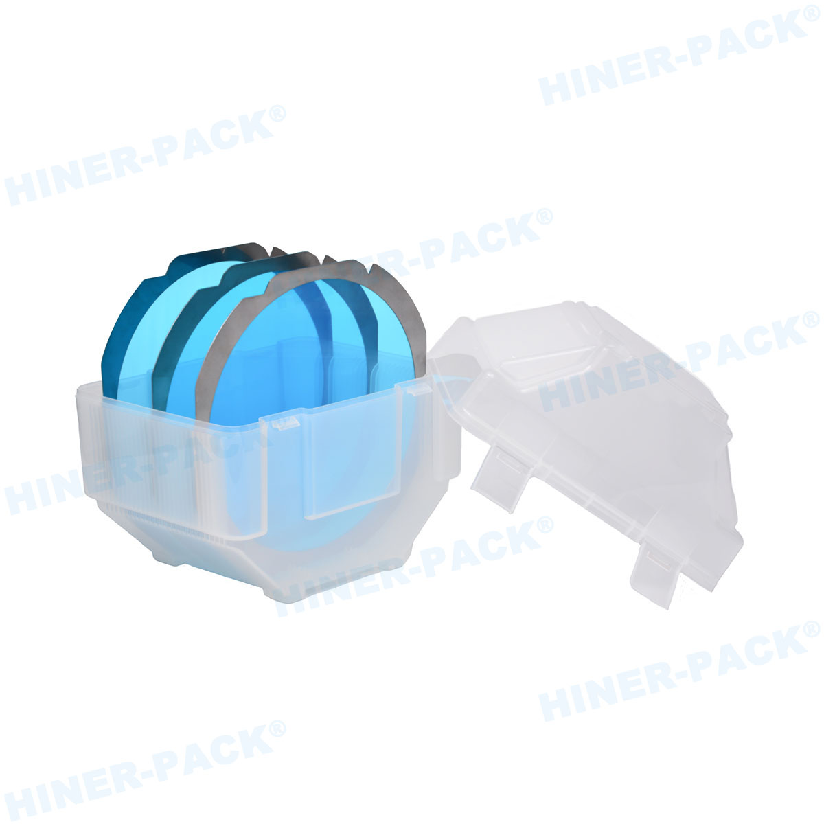
Hiner-pack's Solutions for Particle-Free Wafer Storage
Hiner-pack specializes in wafer storage products. Their systems are engineered for particle-free performance.
They offer a range of containers and cabinets. These products support high-yield semiconductor manufacturing.
Product Features and Benefits
Hiner-pack's storage solutions incorporate advanced features. These ensure contamination control and ease of use.
Key features include:
Sealed designs with gasket mechanisms to block particles.
Compatibility with standard wafer sizes and automation tools.
Materials tested for low particulate generation and chemical resistance.
Integration with Cleanroom Environments
Hiner-pack products are designed for seamless cleanroom integration. They work with existing handling equipment and protocols.
Proper cleanroom engineering decoration enhances storage system effectiveness. This includes layout planning and surface treatments to minimize particle sources.
Best Practices for Maintaining Particle-Free Storage
Implementing particle-free wafer storage requires adherence to best practices. These cover handling, maintenance, and monitoring.
Consistent procedures reduce contamination risks. They extend the life of storage systems.
Handling Procedures for Wafers
Operators must follow strict protocols when accessing wafers. This includes using gloves and cleanroom attire.
Steps to minimize particle introduction:
Limit exposure time when wafers are outside storage.
Use automated handling systems where possible.
Perform operations in certified cleanroom zones.
Maintenance and Cleaning of Storage Systems
Regular maintenance prevents particle buildup. Storage units should be cleaned with approved methods.
Recommended practices:
Schedule periodic inspections for wear and contamination.
Use non-abrasive cleaners and lint-free wipes.
Replace filters and seals according to manufacturer guidelines.
Future Trends in Wafer Storage Technology
The semiconductor industry continuously evolves. Particle-free wafer storage is adapting to new challenges.
Trends include smarter systems and enhanced materials. These developments aim for higher cleanliness levels.
Innovations and Developments
Emerging technologies focus on automation and monitoring. Sensors can detect particle levels in real time.
Advances to watch:
Integration of IoT for predictive maintenance of storage units.
New polymer composites that further reduce particle emission.
Compact designs for next-generation fabrication facilities.
Conclusion: Ensuring Reliability with Particle-Free Wafer Storage
Particle-free wafer storage is essential for semiconductor quality. It safeguards wafers from contamination throughout production.
By adopting robust technologies and practices, manufacturers can improve yields. Hiner-pack's solutions contribute to this goal.
As industry demands grow, particle-free wafer storage will remain a critical focus. Investing in effective systems supports long-term success.
Frequently Asked Questions about Particle-Free Wafer Storage
Q1: What is particle-free wafer storage?
A1: Particle-free wafer storage refers to systems and methods designed to prevent particulate contamination during the storage of semiconductor wafers. It involves using sealed containers, cleanroom-compatible materials, and controlled environments to maintain wafer cleanliness.
Q2: Why is particle-free storage critical for semiconductor manufacturing?
A2: Particles can cause defects in integrated circuits, leading to reduced yields and increased costs. Particle-free storage minimizes contamination risks, ensuring wafers meet quality standards and device performance requirements.
Q3: How do Hiner-pack products support particle-free wafer storage?
A3: Hiner-pack offers storage solutions with features like sealed designs, antistatic materials, and compatibility with cleanroom protocols. Their products are engineered to reduce particle generation and integrate smoothly into semiconductor workflows.
Q4: What role does cleanroom engineering play in wafer storage?
A4: Cleanroom engineering, including proper layout and surface treatments, creates an environment that supports particle-free storage. Effective cleanroom engineering decoration helps control airborne particles and enhances the performance of storage systems.
Q5: How often should wafer storage systems be cleaned and maintained?
A5: Maintenance frequency depends on usage and cleanroom standards. Generally, storage systems should be inspected regularly, with cleaning performed using approved methods. Follow manufacturer guidelines, such as those from Hiner-pack, for optimal schedules.


