
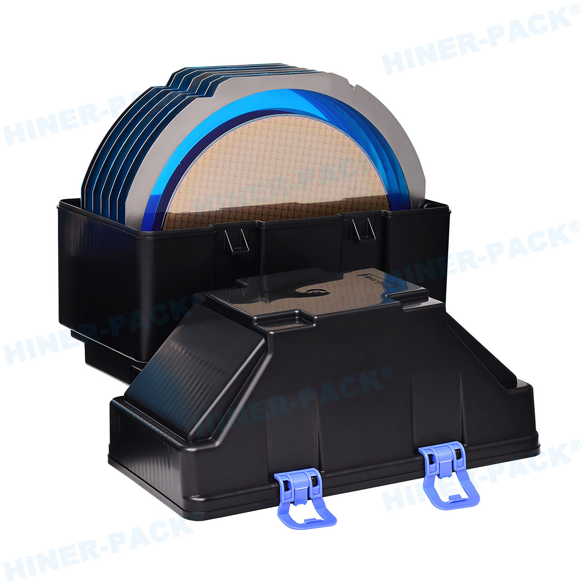
In the pristine, hyper-controlled environment of a semiconductor fab, the most valuable objects are not the multi-million dollar lithography machines. They are the silicon wafers, worth tens of thousands of dollars each, that journey through them. Protecting these exquisite disks of potential is a deceptively simple-looking container: the plastic wafer box. Often called a wafer carrier or cassette, these boxes are the unsung heroes of the semiconductor supply chain, safeguarding trillions of dollars in global electronics production. For manufacturers like Hiner-pack, engineering these plastic wafer boxes is a discipline of precision, materials science, and relentless attention to detail. This article breaks down the five critical functions that make high-quality plastic wafer boxes non-negotiable for modern chip manufacturing.
Beyond Simple Storage: The Multi-Faceted Role of Plastic Wafer Boxes
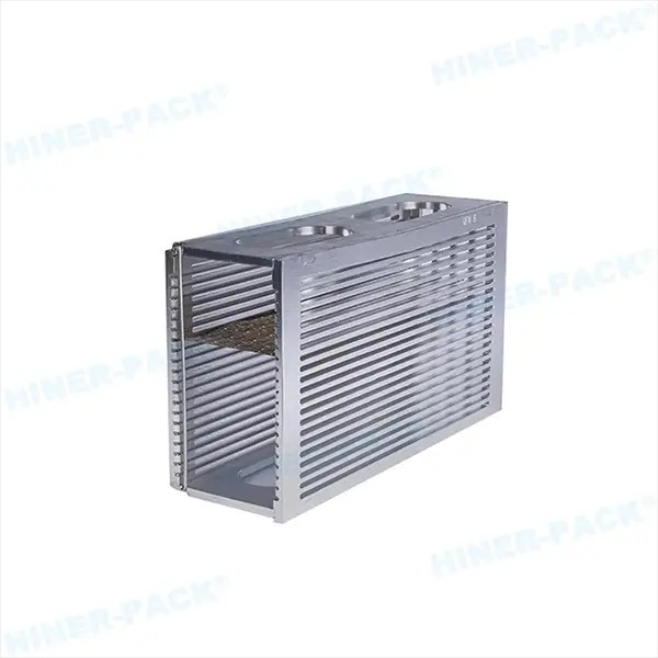
The term "box" can be misleading. It implies a passive container. In reality, a plastic wafer transport carrier is an active, integral component of the manufacturing process. Its design directly influences yield, automation efficiency, and total cost of ownership.
1. The First Line of Defense: Contamination Control
The enemy in a fab is small—microscopically small. Particulate contamination is a primary cause of chip defects and yield loss. High-performance plastic wafer boxes are the first and most constant barrier against this threat.
Low-Particulate Materials: Unlike standard plastics, the advanced polymers used by Hiner-pack are engineered for minimal particle shedding. Through specialized compounding and cleanroom molding processes, the material itself is inherently clean and stable.
Smooth, Rounded Pockets: The internal slots that cradle each wafer are designed with smooth, radii-free contours. This eliminates sharp edges that can generate particles through friction as wafers are inserted or removed.
Sealing Solutions: For wafer shipping containers, a robust sealing mechanism is integrated to create a micro-environment that locks out external contaminants during inter-facility transport.
2. Ensuring Operational Integrity: Mechanical and Dimensional Stability
A plastic wafer cassette must be perfectly rigid and dimensionally consistent. Any warping, flexing, or deviation from standard specifications can have catastrophic consequences.
SEMI Standards Compliance: The entire global semiconductor industry relies on standards set by SEMI. Hiner-pack designs all its plastic wafer boxes to exact SEMI specifications (e.g., SEMI E1.2, E15.1, E47.1). This ensures they interface flawlessly with equipment from any manufacturer—be it an ASML scanner, an Applied Materials etcher, or a Tokyo Electron deposition tool.
Robustness for AMHS: These boxes must withstand constant movement by robotic arms, automated guided vehicles (AGVs), and overhead hoist transport systems (OHTs). Their structural integrity prevents misloading, jams, and costly system downtime.
3. Neutralizing an Invisible Threat: Electrostatic Discharge (ESD) Protection
A static spark, imperceptible to a human, can easily destroy the nanoscale transistors on a wafer. Plastic wafer boxes address this through material science.
Static-Dissipative Properties: Hiner-pack utilizes plastics like static-dissipative polycarbonate (PC) or PEEK. These materials prevent the buildup of static charge by allowing it to slowly and safely dissipate, effectively creating a Faraday cage for the wafers inside.
4. Surviving the Process Environment: Chemical and Thermal Resistance
Wafers often enter and exit process tools while still housed in their carrier. This means the plastic wafer box can be exposed to chemical splashes, aggressive plasma byproducts, and high temperatures during cleaning cycles.
Resistant Polymers: Materials are selected specifically for their resistance to common fab chemicals like SC-1 and SC-2 cleaning solutions, solvents, and acids. This prevents the carrier from degrading, clouding, or leaching contaminants back onto the wafers.
5. Enabling the Smart Fab: Integration with Industry 4.0
The modern fab is a data-rich environment. The humble plastic wafer box has evolved to be a key data carrier.
RFID Integration: Hiner-pack designs boxes with dedicated, recessed pockets for RFID tags. These tags allow the wafer lot to be identified and tracked automatically throughout its entire manufacturing journey, enabling full traceability and streamlined manufacturing execution systems (MES).
Hiner-pack's Engineering Philosophy: Where Precision Meets Durability
At Hiner-pack, we don't just mold plastic; we engineer critical process components. Our approach to manufacturing plastic wafer boxes is built on three pillars:
Material Purity and Selection: We start with certified, high-purity polymer grades from leading suppliers. We understand the nuanced differences between, for example, a standard PC and a PC-ISO suitable for medical-grade or high-end semiconductor applications, ensuring optimal performance for the client's specific use case.
Precision Injection Molding: Our molding presses operate in controlled environments to maintain cleanliness. We use high-precision molds crafted from tool-grade steel, which are meticulously maintained to ensure every batch of plastic wafer boxes meets sub-millimeter accuracy.
Rigorous Quality Assurance: Every single Hiner-pack carrier undergoes a multi-point inspection. We check for critical dimensions, visual defects, and mechanical function. This commitment to quality ensures that when you use a Hiner-pack plastic wafer shipping container, you can be confident in its performance.
The Future of Wafer Packaging
The evolution of plastic wafer boxes continues. As chips advance, so do their packaging needs. Trends we are actively engaged in include:
Carriers for Advanced Materials: Developing boxes for larger 450mm wafers, as well as specialized carriers for more fragile materials like GaAs and SiC wafers.
Intelligent Carriers: Integrating more sophisticated sensors directly into the carrier body to monitor parameters like humidity, tilt, and shock in real-time.
Sustainability: Exploring closed-loop recycling programs and bio-based polymers to reduce the environmental footprint of our products without compromising performance.
Frequently Asked Questions (FAQs)
Q1: What is the main difference between a FOUP and a standard plastic wafer box?
A1: A FOUP (Front-Opening Unified Pod) is a specific type of plastic wafer box designed for 300mm wafers. It is a sealed, front-opening pod that maintains a mini-environment of inert gas (like N2) around the wafers. Standard plastic wafer cassettes for 200mm and smaller wafers are typically open structures used within the controlled environment of the cleanroom itself.
Q2: How do I know if a plastic wafer box is compatible with my equipment?
A2: Compatibility is determined by SEMI standards. You should check the specific standard your equipment requires (e.g., SEMI E1.2 for 150mm carriers). Hiner-pack provides full compliance documentation for all our plastic wafer boxes, guaranteeing they meet the mechanical and dimensional specs for interoperable use.
Q3: Can Hiner-pack's plastic wafer boxes be used for long-term wafer storage?
A3: Yes, absolutely. Our boxes are manufactured from high-purity, chemically stable polymers that will not outgas or degrade over time, making them ideal for safe, long-term storage in automated stockers or cleanroom cabinets.
Q4: What is the recommended cleaning procedure for these boxes?
A4: We recommend following SEMI guideline E82 for carrier cleaning. Typically, this involves using a specialized, low-residue cleaning solution in a dedicated cleaning tool, followed by a thorough DI water rinse and a particle-free drying process. Manual cleaning is generally discouraged due to the high risk of contamination and damage.
Q5: Do you offer custom-designed plastic wafer shipping containers?
A5: Yes, Hiner-pack has a dedicated engineering team for custom solutions. We can work with you to design a plastic wafer shipping container with specific features, such as unique RFID tag locations, custom latching mechanisms, or tailored material compositions for unique process requirements.


