
In the highly precise world of semiconductor manufacturing, every nanometer counts. The journey of a silicon wafer from a bare substrate to a complex integrated circuit involves hundreds of steps, each requiring the utmost protection from contaminants and physical damage. At the heart of this logistical ballet is a seemingly simple yet critically important tool: the plastic wafer transport carrier. Far from being just a box, this carrier is a first line of defense, a key to automation, and a significant factor in overall yield. This article delves into why the plastic wafer transport carrier has become an indispensable asset in fabs worldwide and how companies like Hiner-pack are engineering them for the future.
Why the Shift to Plastic Wafer Carriers?
For decades, the semiconductor industry relied heavily on carriers made from materials like polycarbonate or metals. However, as process nodes shrank to 5nm and below, the limitations of these materials became apparent. The modern plastic wafer transport carrier, often made from advanced engineering thermoplastics like PEEK (Polyether Ether Ketone) or PC (Polycarbonate) composites, addresses these critical challenges.
Contamination Control: Today's fabs are ultra-clean environments. Traditional materials could shed particles through friction or outgas volatile chemicals, leading to yield-killing defects. Advanced plastic wafer carriers are designed with low-particle generation and low-outgassing properties, ensuring they protect, rather than threaten, the wafers inside.
Electrostatic Discharge (ESD) Protection: Static electricity can instantly destroy sensitive microchips. Modern carriers are manufactured from static-dissipative or conductive plastics, safely channeling any electrostatic charge away from the wafers.
Chemical Resistance: Wafer fabrication involves exposure to harsh chemicals and plasma during cleaning and etching processes. The high-performance polymers used in carriers like those from Hiner-pack are engineered to withstand these aggressive environments without degrading, warping, or contaminating the process tools.
Key Design Features of a High-Performance Plastic Wafer Carrier
Not all plastic wafer shipping boxes are created equal. Their design is a result of meticulous engineering focused on four core areas:
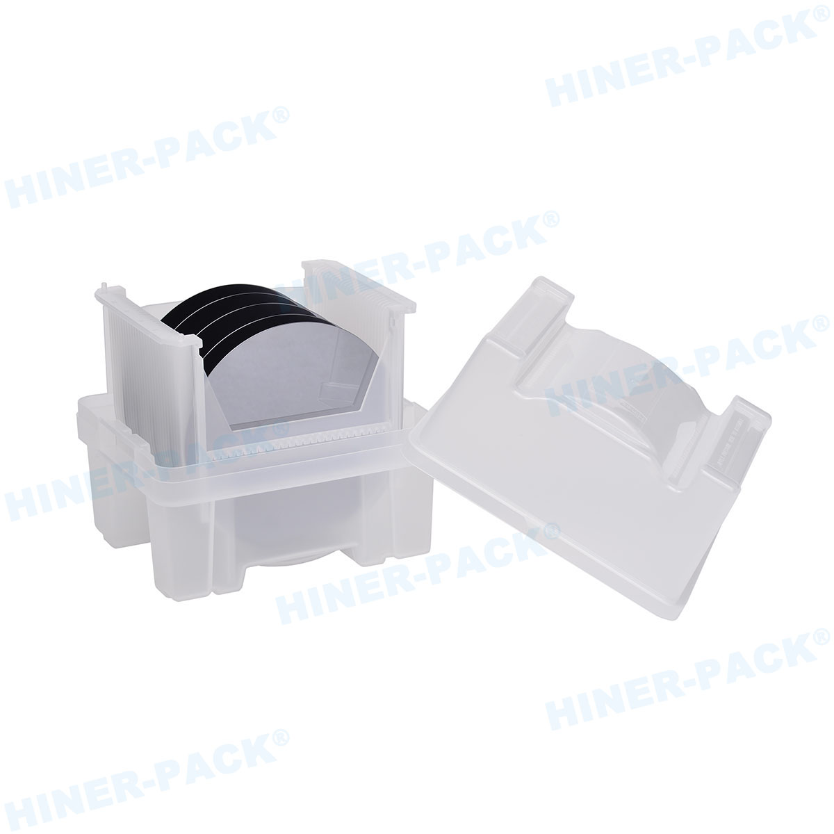
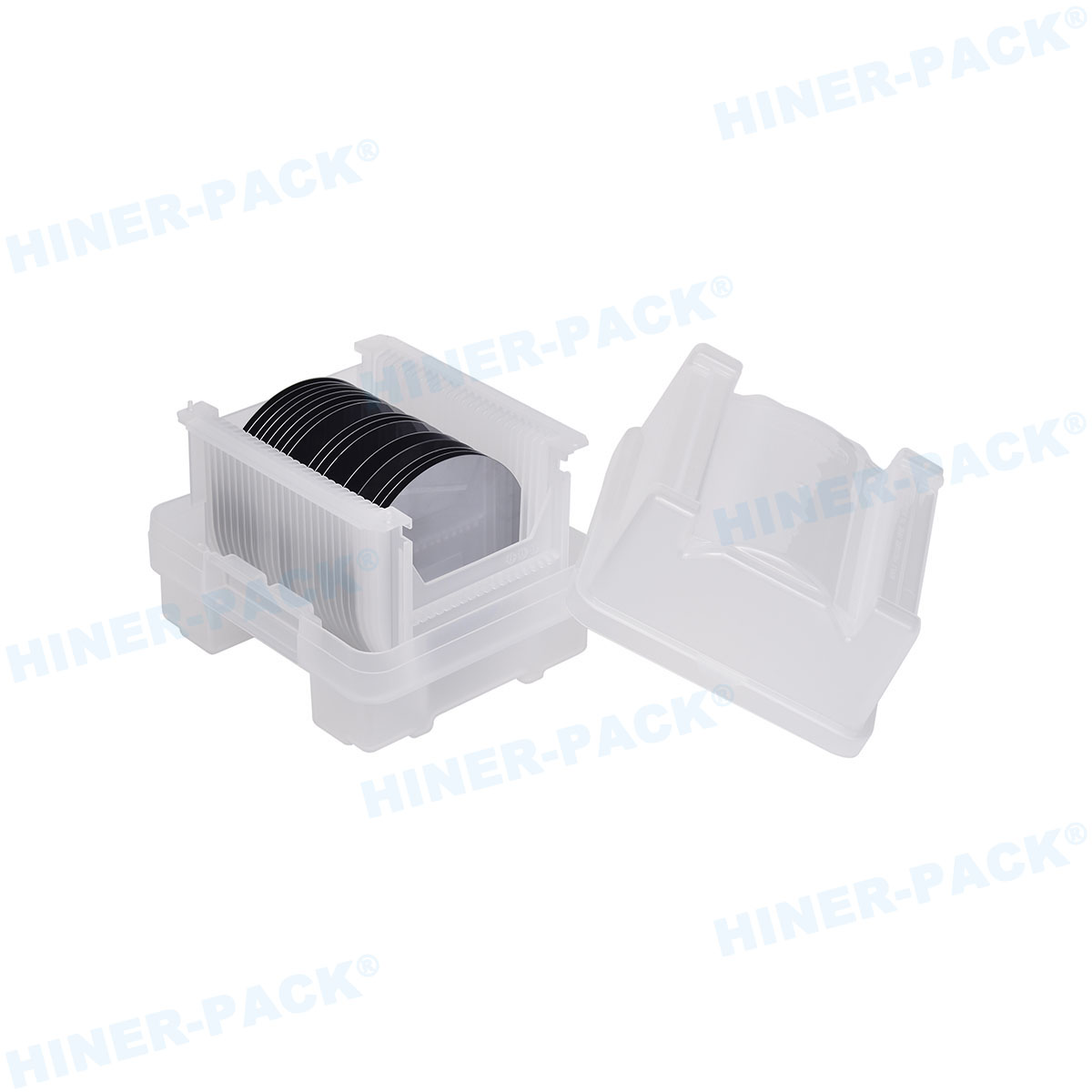
Precision Pocket Geometry: Each slot that holds a wafer is machined to exact tolerances. This prevents wafer movement during transit, minimizing mechanical stress and the risk of micro-cracking. The smooth, rounded contours of the pockets also drastically reduce the potential for particle generation.
Mechanical Robustness and Lightweight Nature: Despite their precision, these carriers must be durable enough to withstand the rigors of automated material handling systems (AMHS). High-quality plastic wafer transport carriers offer an excellent strength-to-weight ratio. This reduces strain on robotic arms and makes manual handling safer and more ergonomic for operators.
RFID and Tracking Integration: In an Industry 4.0 fab, traceability is non-negotiable. Carriers are now designed with embedded slots or areas for RFID tags, allowing for seamless tracking of wafer lots through every stage of production. This data is crucial for process control and inventory management.
Standardized Footprints (SEMI Compliance): Interoperability is key. Carriers adhere to strict SEMI standards, ensuring they fit perfectly into processing tools, stockers, and automated guided vehicles (AGVs) from different equipment manufacturers. This standardization, enabled by precisely molded plastic materials, is the glue that holds fab automation together.
Applications Across the Semiconductor Lifecycle
The use of the plastic wafer transport carrier extends beyond the fab floor.
In-Fab Transport: Moving wafer lots between photolithography, etching, deposition, and inspection tools.
Wafer Storage: Safely housing wafers in automated stockers for extended periods.
Inter-Bay and Intra-Bay Logistics: Facilitated by AMHS, where carriers are shuttled between different cleanroom bays.
Shipping and Logistics: For transporting wafers between different company fabs or to outsourcing partners for assembly and test. Rugged, sealable plastic wafer shipping boxes are essential for this purpose.
Hiner-pack's Approach to Advanced Wafer Carrier Solutions
At Hiner-pack, we understand that a carrier is more than a container; it's a critical process component. Our plastic wafer transport carriers are developed with a focus on:
Material Science Expertise: We select and compound proprietary polymer blends to achieve the optimal balance of low particulation, high chemical resistance, and long-term dimensional stability.
Precision Molding: Our state-of-the-art injection molding facilities ensure that every carrier and every wafer pocket meets the most stringent SEMI specifications, batch after batch.
Customization for Specific Needs: We work with customers to develop custom carriers for unique applications, such as those for fragile compound semiconductor wafers or specialized MEMS devices.
By focusing on these core principles, Hiner-pack ensures that our plastic wafer boxes contribute directly to our customers' yield management and operational efficiency goals.
The Future: Smarter Carriers for Smarter Fabs
The evolution of the plastic wafer transport carrier is far from over. The next generation will feature:
Integrated Sensors: Carriers with built-in sensors to monitor internal conditions like temperature, humidity, and vibration in real-time, providing a "health report" for the wafer lot.
Advanced Materials for New Challenges: As new materials like silicon carbide (SiC) and gallium nitride (GaN) gain prominence, carriers will need to be adapted to handle their unique properties and thicker profiles.
Enhanced Data Carriers: Moving beyond simple identification to storing critical process data directly on the carrier itself, creating a truly integrated manufacturing flow.
Frequently Asked Questions (FAQs)
Q1: Why are plastic wafer carriers preferred over traditional metal ones?
A1: Plastic wafer transport carriers are preferred primarily for their superior contamination control. They generate fewer particles, do not corrode, and can be formulated to prevent electrostatic discharge. They are also lighter, reducing load on automation systems, and offer better chemical resistance to the harsh cleansers used in fab processes.
Q2: How often should a plastic wafer transport carrier be cleaned and inspected?
A2: The cleaning and inspection frequency depends on the carrier's usage and the specific fab's cleanliness protocols. Typically, carriers undergo a rigorous cleaning process after a certain number of cycles or if monitoring indicates a rise in particle counts. Regular visual and automated inspections for physical damage, such as cracked pockets or wear, are also a standard part of preventative maintenance.
Q3: Can Hiner-pack's plastic wafer carriers withstand high-temperature processes?
A3: Yes, many of our carriers are manufactured from high-temperature thermoplastics like PEEK or advanced PCTG, which can withstand the elevated temperatures encountered in certain process tools and cleaning procedures without warping or degrading. It is crucial to select the carrier material that matches your specific thermal requirements.
Q4: What is the typical lifespan of a high-quality plastic wafer box?
A4: The lifespan varies based on the material, the aggressiveness of the process environments, and handling conditions. A well-maintained carrier from a quality manufacturer like Hiner-pack can last for several years and thousands of cycles before needing replacement. Proper cleaning and handling are key to maximizing longevity.
Q5: Are Hiner-pack carriers compatible with all major AMHS and stocker systems?
A5: Absolutely. Hiner-pack designs and manufactures all our plastic wafer transport carriers to meet relevant SEMI standards. This ensures mechanical compatibility with the vast majority of automated material handling systems, FOUP/LP load ports, and stockers from leading equipment suppliers globally.


