
In semiconductor front-end and back-end manufacturing, the safe storage and transport of bare silicon wafers demand carriers that balance physical protection, electrostatic discharge (ESD) control, and ultralow particle shedding. PP wafer boxes – injection molded from virgin polypropylene – have become a standard solution for 150 mm, 200 mm, and 300 mm wafer handling in fab cleanrooms and assembly areas. This article provides a component-level analysis of PP wafer boxes, covering material grades, slot pitch precision, chemical resistance, and compatibility with automated wafer transfer systems. Drawing on data from Hiner-pack‘s 15+ years of wafer carrier manufacturing, we will examine how to select the correct box for your wafer diameter, thickness, and process step (e.g., diffusion, inspection, or shipping).
1. Why Polypropylene for Wafer Carriers? Material Science Basis
Polypropylene (PP) is the dominant material for PP wafer boxes because of its intrinsic properties:
Low particle generation: PP exhibits low abrasion compared to PVC or ABS. Sliding wear tests show PP produces < 0.2 particles/cm² per 1000 cycles (SEMI E46 compliant).
ESD-safe without additives: Static decay time for virgin PP is > 10 seconds, but carbon-filled or inherently dissipative (ID) PP grades achieve 10⁶–10⁹ Ω surface resistivity. This prevents charge buildup without sloughing conductive particles.
Chemical resistance: PP resists acids (HF, H₂SO₄), bases (NH₄OH), and common solvents (isopropanol, acetone) used in wafer cleaning. No surface degradation after 24-hour immersion in SPM (H₂SO₄+H₂O₂) at 120°C.
High purity: No plasticizers, halogens, or heavy metals. Outgassing (by GC-MS) shows only trace levels of propylene monomer (< 0.01 µg/g).
Compared to PFA or PTFE, PP wafer boxes offer a lower cost (40–60% less) while meeting Class 1 cleanroom requirements (ISO 14644-1). Hiner-pack uses only FDA-grade, ultra-pure PP pellets with double-bagging and vacuum sealing to prevent contamination before molding.
2. Key Design Parameters for PP Wafer Boxes
Selecting the correct PP wafer boxes requires attention to five engineering specifications.
2.1 Wafer Diameter and Slot Pitch
Standard boxes accommodate 150 mm (6 inch), 200 mm (8 inch), or 300 mm (12 inch) wafers. Slot pitch – the vertical distance between adjacent wafer slots – must match the wafer thickness plus clearance for robot end effectors.
For 150 mm wafers (thickness 0.675 mm): slot pitch 4.76 mm (3/16 inch) is common.
For 200 mm wafers (0.725 mm): pitch 6.35 mm (1/4 inch) or 10 mm for thicker substrates.
For 300 mm wafers (0.775 mm): pitch 10 mm or 12.7 mm, often with wafer spacing guides to prevent edge contact.
Slot width tolerance must be ±0.05 mm to avoid wafer sticking or rattling. PP wafer boxes from Hiner-pack include molded-in slot identifiers (A, B, C) for batch traceability.
2.2 Cleanroom Compatibility and Outgassing
For use in lithography or deposition areas, boxes must meet SEMI E78 (outgassing) and E46 (particle) standards. Virgin PP emits low levels of hydrocarbons (C10–C20), but for sensitive processes (e.g., EUV), carbon-filled PP is replaced with conductive PP copolymer that has reduced outgassing. Hiner-pack provides outgassing test reports per SEMI E108 for each lot of PP wafer boxes.
2.3 Mechanical Strength and Stackability
Box walls must resist bowing when stacked 10 high (typical load 50 kg). Ribbed sidewalls and corner gussets increase column strength. A well-designed 25-slot box for 200 mm wafers withstands 80 kg static load without permanent deformation. The latch mechanism – usually a snap-fit or rotating clip – must survive 10,000 open-close cycles without particle generation.
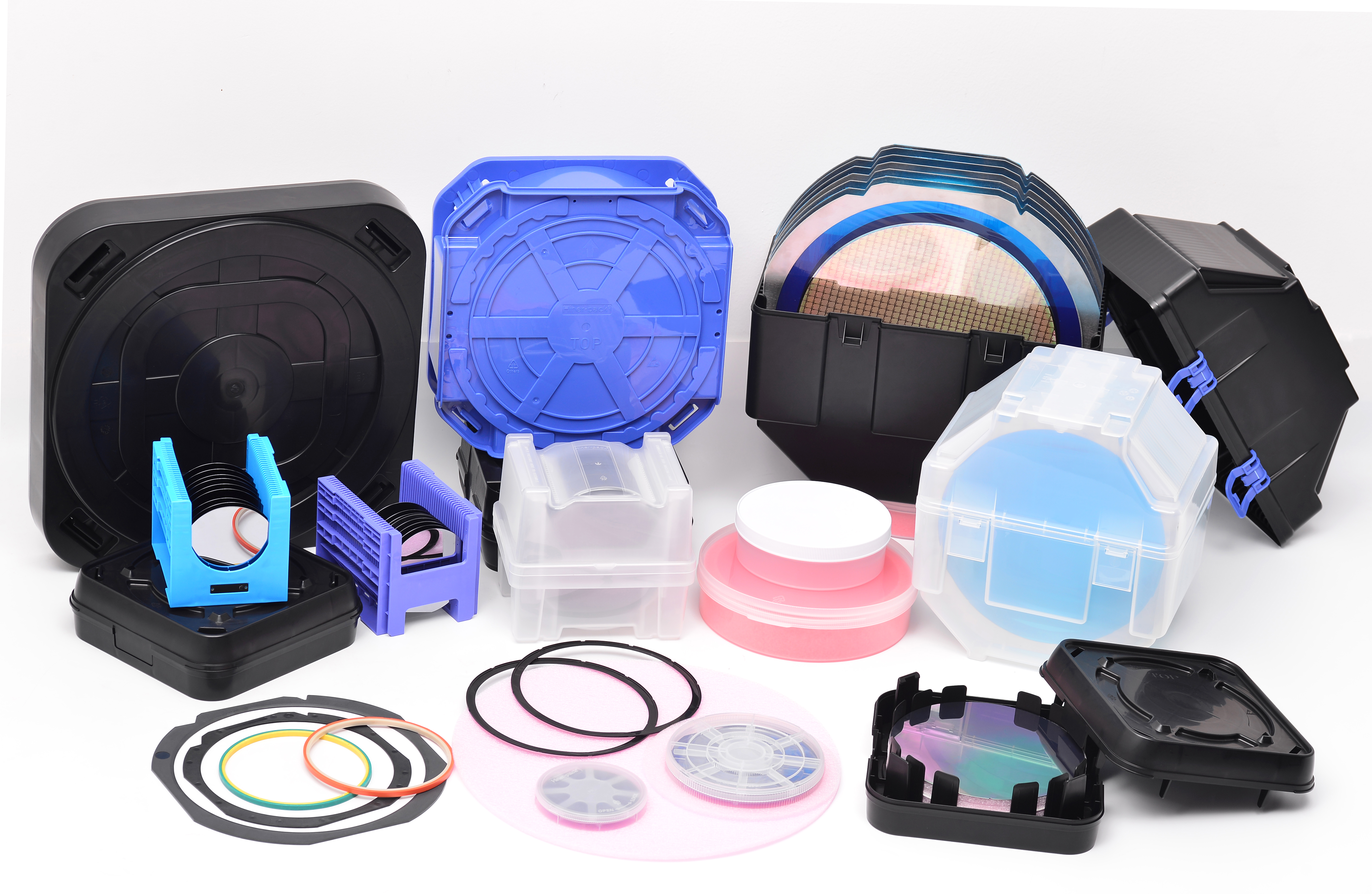
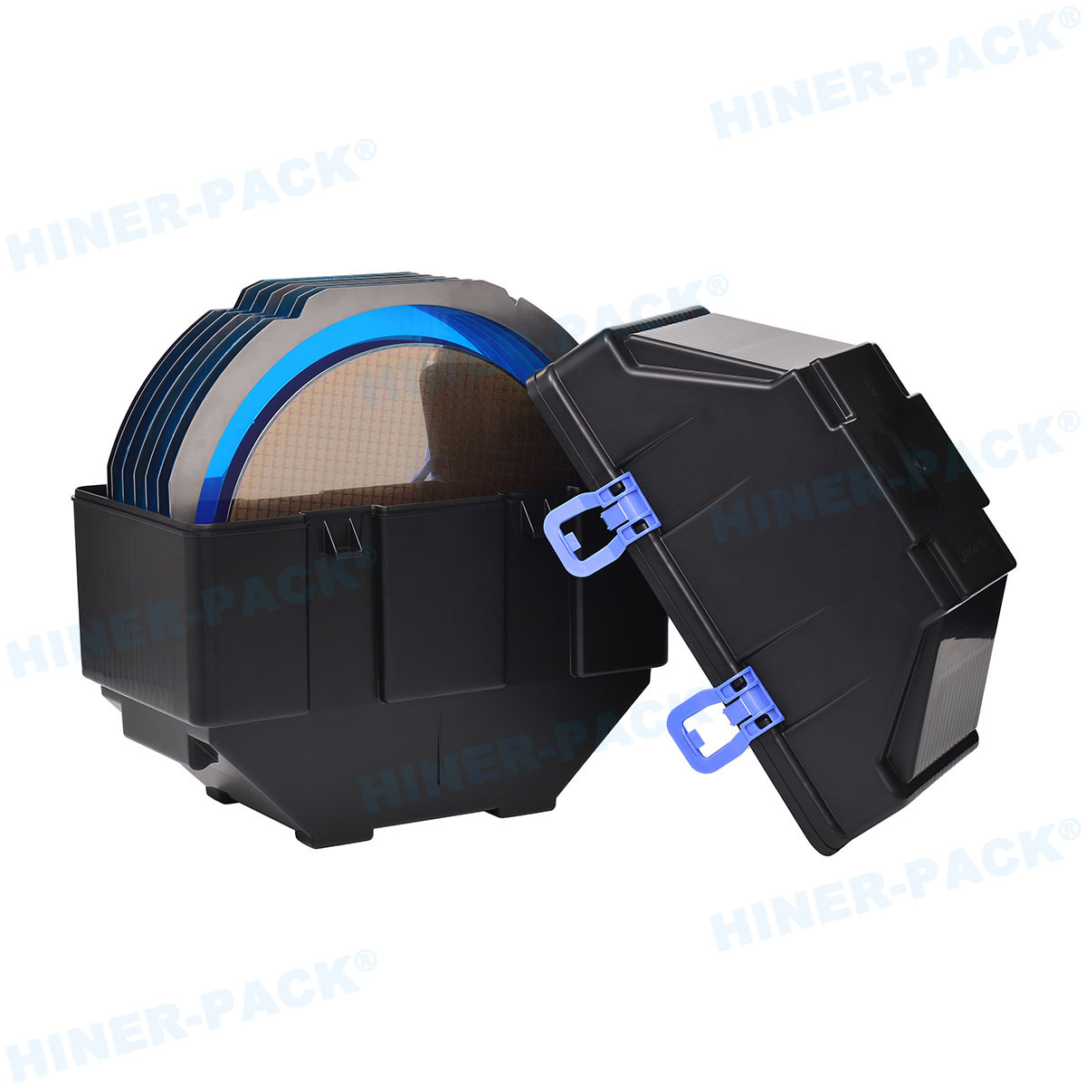
3. Types of PP Wafer Boxes by Application
Different process steps require different configurations.
Standard shipper boxes: For inter-fab or inter-company transport. Include foam inserts or gel packs for vibration damping. Compliant with SEMI G72 (shock resistance).
Process boxes (in-fab): Open design with ventilation slots for gas flow during bake-out or cleaning cycles. Often used in wet benches and furnaces.
Low-particle (LP) boxes: Double-shot molded with smooth slot surfaces; particle levels < 10 particles > 0.1 µm per wafer after 10 cycles (SEMI E46).
High-temperature boxes: Made from heat-stabilized PP (with antioxidant) for use up to 135°C continuous (e.g., post-CMP bake). Standard PP distorts above 110°C.
Hiner-pack offers all four types, with color coding (white, blue, black, anti-static pink) to differentiate process steps and prevent cross-contamination.
4. Industry Pain Points and Engineering Solutions
Despite standardized designs, wafer fabs face recurring issues with PP wafer boxes. Below are three common failure modes and their remedies.
Wafer edge chipping: Caused by rough slot surfaces or misaligned guide ribs. Solution – use electropolished mold inserts to achieve surface roughness Ra < 0.2 µm. Hiner-pack uses nickel-coated cavities for mirror-finish slots.
Static charge buildup during automated opening: Robots that open box lids at high speed ( > 0.5 m/s) can generate triboelectric charges > 2 kV, potentially damaging gate oxides. Remedy – specify dissipative PP with surface resistivity 10⁵–10⁹ Ω, plus grounding tabs that contact the load port ground pin.
Bacteria or mold growth in wet storage: When boxes are stored after wet processing without drying, moisture allows microbial growth. Solution – use silver-ion embedded PP (antimicrobial grade) or ensure boxes are dried in nitrogen purge cabinets before storage.
According to Hiner-pack's field data, these solutions reduce wafer breakage by 60–80% and electrical failures related to ESD by 45%.
5. Compatibility with Automated Material Handling Systems (AMHS)
Modern 300 mm fabs use overhead hoist transport (OHT) and load ports that require PP wafer boxes to conform to SEMI E15.1 (specifications for mechanical interfaces). Critical dimensions include:
Bottom kinematic coupling plate: Three precision grooves (1.5 mm depth, 120° apart) for OHT gripper alignment.
RFID pocket: Size and location for a 13.56 MHz tag (ISO 15693) that stores wafer lot ID and process history.
Lid grip features: Two recessed handles that allow robot end effectors to lift the lid vertically without tilting.
Non-standard boxes that deviate from SEMI dimensions cause jamming and sensor errors. PP wafer boxes from Hiner-pack are certified to pass 10,000 cycles on a standard load port without wear exceeding 0.1 mm.
6. Cleaning and Reuse Protocols for PP Wafer Boxes
To reduce cost per wafer, fabs clean and reuse PP wafer boxes multiple times. However, improper cleaning degrades the material. Recommended cleaning procedure per SEMI E49:
Pre-rinse with DI water (18 MΩ·cm) at 50°C for 2 minutes.
Ultrasonic cleaning in 2% surfactant (e.g., Triton X-100) at 40 kHz, 5 minutes.
DI water cascade rinse (3 tanks) for 3 minutes total.
Hot air drying at 60°C for 20 minutes (oven) or nitrogen blow-off.
Final particle test (liquid particle counter) – must show < 50 particles > 0.2 µm per 100 cm².
Avoid using strong alkalis (pH > 12) or solvents like xylene, which can craze PP. Boxes reused more than 50 cycles should be inspected for slot wear using a borescope. Hiner-pack offers a recycling program where worn boxes are ground and remolded into new boxes (closed-loop recycling).
7. Regulatory and Quality Certifications
Suppliers of PP wafer boxes to tier-1 fabs must provide documentation for:
ISO 9001:2015 (quality management)
ISO 14644-1 Class 5 (cleanroom manufacturing)
SEMI E78-0998 (outgassing test)
SEMI E46-0301 (particle performance)
RoHS 3 (2015/863/EU) – no restricted substances
REACH SVHC compliance
Hiner-pack maintains a certified Class 10,000 (ISO 7) cleanroom for molding and assembly, with particle counters monitoring each production batch. Lot traceability allows recall of any box to its raw material batch.
8. Frequently Asked Questions (FAQ) – PP Wafer Boxes
Q1: What is the typical lifespan of a PP wafer box under normal fab
use?
A1: With proper cleaning and handling, a
high-quality PP wafer box can last 3–5 years (200–300 cycles).
After 500 cycles, slot wear may exceed 0.1 mm, risking wafer edge contact.
Hiner-pack boxes are rated for 400 cycles with particle performance
guarantee.
Q2: Can PP wafer boxes be used for wafer storage in acid environments
(e.g., wet etch benches)?
A2: Yes, PP is resistant
to most acids (HF, HNO₃, HCl) up to 30% concentration at room temperature.
However, for concentrated H₂SO₄ (> 70%) or hot acids (> 60°C), use PFA or
PTFE carriers. Hiner-pack provides chemical compatibility charts upon
request.
Q3: Are conductive PP wafer boxes necessary for all
applications?
A3: No. For wafers with feature sizes
> 90 nm, standard antistatic PP (surface resistivity 10⁹–10¹¹ Ω) is
sufficient. For < 28 nm nodes, dissipative PP (10⁶–10⁹ Ω) is recommended to
prevent charge-induced damage. For handling of MEMS or GaAs wafers, conductive
PP (< 10⁵ Ω) is required.
Q4: How do I verify the cleanliness of a new batch of PP wafer
boxes?
A4: Request a lot certificate from the
supplier including particle counts per SEMI E46 (extraction method) and
outgassing per SEMI E78. For critical applications, perform an ion
chromatography (IC) test on a sample box to verify fluoride, chloride, and
sulfate ions are below 0.1 µg/g.
Q5: Can PP wafer boxes be autoclaved for
sterilization?
A5: Standard PP distorts at 121°C
(autoclave temperature). Use high-temperature PP (glass-filled or
heat-stabilized) rated for 135°C. However, autoclaving accelerates oxidation –
limit to 10 cycles. For sterile applications, gamma irradiation (25–50 kGy) is
preferred as it does not soften PP.
Q6: What is the maximum number of wafers a single PP wafer box can
hold?
A6: Standard boxes hold 25 wafers (for 200
mm) or 13 wafers (for 300 mm). Custom boxes can be molded with 50 slots for 150
mm wafers, but handling becomes difficult. Hiner-pack's maximum is 50 slots for
150 mm, 25 slots for 200 mm, and 25 slots for 300 mm (extra-deep design).
9. Select the Right PP Wafer Box for Your Process Node
Choosing the correct PP wafer boxes involves matching material grade, slot precision, and ESD protection to your wafer diameter, feature size, and process chemistry. Generic boxes from non-specialized suppliers often lack SEMI certifications or cleanroom manufacturing, leading to yield loss.
Hiner-pack offers a complimentary engineering review including:
Material selection guide (virgin PP, conductive PP, or high-temperature PP).
Slot pitch optimization for thin wafers (down to 0.1 mm thickness).
Custom RFID pocket design and in-mold labeling.
Sample boxes for particle testing in your fab.
Request your quotation today – provide your wafer diameter, thickness, process steps (e.g., etch, CMP, inspection), and annual volume. Our cleanroom engineering team will respond within 2 business days with a specification sheet and sample pricing. Click here to contact Hiner-pack’s semiconductor packaging specialists or call+86 755 2322 9236 for immediate assistance.


