In semiconductor manufacturing, the journey of a silicon wafer from bare
substrate to fully processed die involves hundreds of process steps. Throughout
this flow, the wafer carrier
manufacturer provides the fundamental hardware that safeguards each wafer
against contamination, mechanical damage, and electrostatic discharge. While
often overlooked, the design, material purity, and dimensional precision of
wafer carriers directly influence die yield, especially in advanced nodes and
heterogeneous integration.
This article delivers a deep technical examination of wafer carrier
specifications, application-specific requirements, and engineering solutions for
modern fabs, assembly houses, and OSATs. As an industry expert with two decades
of experience in wafer handling and packaging, I will break down the criteria
that separate commodity trays from high-performance process carriers. Hiner-pack has been at the
forefront of custom carrier engineering, aligning with these stringent
demands.
1. Material Science and ESD Performance: Core Differentiators for Process
Carriers
Not all wafer carriers are equivalent. The base polymer—whether PEEK, PFA,
PEI, or conductive polycarbonate—determines chemical resistance, thermal
stability, and outgassing profiles. For front-end-of-line (FEOL) applications,
carriers must withstand aggressive solvents and elevated temperatures up to
250°C without warping or releasing volatile compounds. Meanwhile, back-end
processes such as wafer-level chip-scale packaging (WLCSP) and fan-out
wafer-level packaging (FOWLP) require static-dissipative carriers to prevent
ESD-induced gate oxide damage.
Leading wafer carrier
manufacturer solutions incorporate carbon nanotube or permanent antistatic
additives achieving surface resistivity between 10⁵–10¹¹ Ω/sq. This range
prevents triboelectric charging while avoiding metallic contamination. For
high-temperature processes like polyimide curing or reflow simulation, PEEK
carriers with low extractable ions (below 10 ppb) are specified. The table below
highlights key material criteria:
Thermal performance: Continuous use temp up to 260°C
(PEEK), short-term peaks to 300°C.
Chemical compatibility: Resistance to NMP, PGMEA, TMAH, and
buffered oxide etch (BOE).
Particle generation: ≤ 0.1 particles/cm² for class 100
cleanroom compatibility.
Outgassing: Meets SEMI S2/S8 and ISO 14644-14 for molecular
contamination.
Advanced injection molding combined with CNC post-processing ensures pocket
depths, edge clearances, and coplanarity are maintained within ±25 µm. An
improperly fitted carrier leads to wafer edge chipping or misalignment during
automated handling—reasons why fabs audit carrier suppliers rigorously.
2. Application-Specific Carrier Architectures: From Bulk Transport to Thin
Wafer Processing
Wafer carriers are not a monolithic category. Based on the application
environment, they are divided into shipping carriers, process carriers, and
storage cassettes. Each must address distinct mechanical stresses and
cleanliness levels.
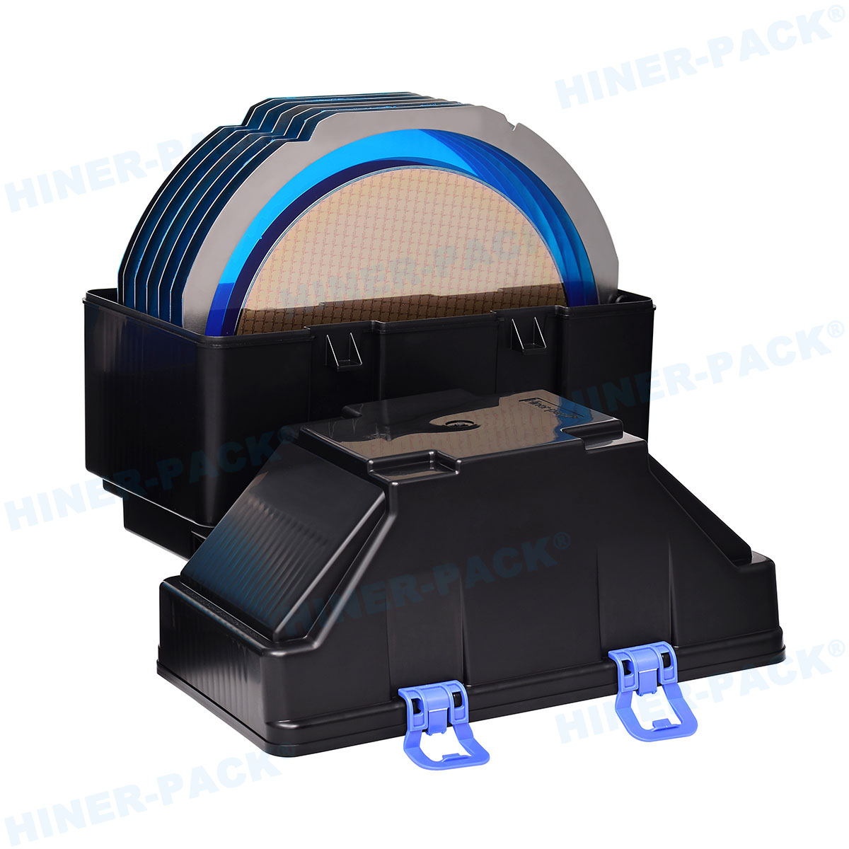
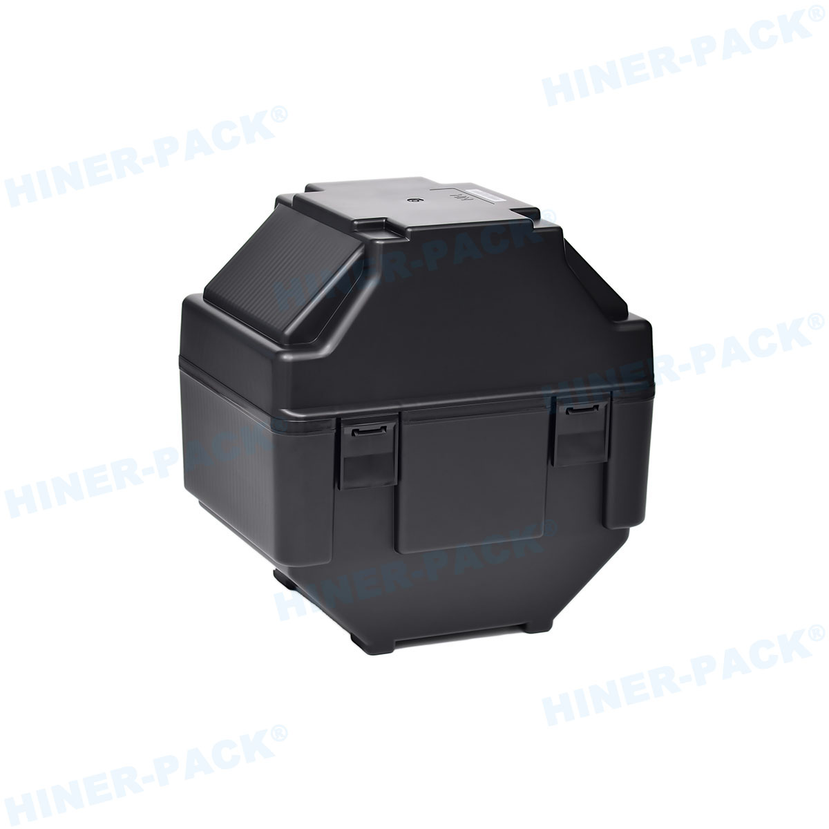
2.1 High-volume shipping carriers (HVM shipping trays)
Designed for inter-fab and international logistics, these carriers must
absorb vibration and thermal fluctuations. They often feature interlocking lids
and foam inserts, but for sensitive 300mm wafers, rigid injection-molded
carriers with cushioning ribs are preferred. A credible wafer carrier
manufacturer provides moisture-barrier packaging options and RFID tagging
for traceability.
2.2 Process carriers for wet etching and plating
Wet benches require carriers with open geometries to allow chemical flow and
drainage. Carrier designs include vertical slots with minimal contact area
(point contact to reduce shadow effects). For silicon interposers and MEMS
devices, carriers integrate fences to prevent wafer floatation. Material choice
shifts to PTFE or PFA for concentrated HF or KOH baths, ensuring no metal
leaching.
2.3 Thin-wafer handling rings and support frames
With wafer thinning down to 30–50 µm for 3D-IC and stacked memory,
traditional carriers cannot prevent warpage or breakage. Here, carriers take the
form of dicing rings bonded with UV tapes or temporary bonding carriers using
adhesive. However, for non-taped handling, specialized thin-wafer carriers with
edge-gripping mechanisms and vacuum grooves are used. These require exceptional
flatness (≤10 µm) and low surface roughness (Ra < 0.8 µm).
Specialty manufacturer Hiner-pack offers engineering
consultation to convert thin-wafer requirements into tool-ready carrier designs,
including automated handling fiducials.
3. Industry Pain Points: Contamination, Cross-Slot Cracks, and Carrier
Lifecycle Management
Despite robust specifications, semiconductor fabs face recurring obstacles
with wafer carriers. Solving these requires deep collaboration between process
engineers and the carrier supplier.
Particle shedding from carrier wear: Repeated processing
cycles and carrier-to-slot friction generate submicron particles that deposit on
wafer backsides, causing focus errors in lithography. Solution: Use lubricious
polymers (e.g., PEEK with internal lubricant) and design slot ribs with rounded
edges.
Electrostatic charge accumulation during automation: Standard carriers allow charge buildup when wafers are robotically transferred.
ESD events can destroy gate oxides. Mitigation: Specify carriers with volume
resistivity 10⁶–10⁹ Ω·cm and integrate ground pins.
Cross-slot wafer cracking: Carriers that lack precision
slot pitch cause wafer edges to contact adjacent slots during thermal expansion.
Simulation-driven design can optimize pitch and incorporate expansion gaps.
Cross-contamination from previous batches: Carriers used
for multiple process steps (e.g., Cu plating then oxide etch) must undergo
validated cleaning. However, porous materials or rough finishes trap residues.
Advanced carriers feature closed-cell surfaces and are
cleanroom-compatible.
Professional wafer carrier
manufacturer services include designing cleanable geometries and providing
baseline contamination test reports per SEMI E45. The best suppliers also offer
a requalification program for carriers after extended use.
4. Selecting a Wafer Carrier Manufacturer: Technical Audit Criteria
When evaluating potential partners, procurement and engineering teams must go
beyond price. The following audit checklist aligns with semiconductor industry
best practices:
Material traceability and batch-to-batch consistency: ISO
9001:2015 with lot-level testing for ash content, metal traces, and resistivity
drift.
Metrology infrastructure: In-house CMM, optical
comparators, and surface roughness testers to verify each cavity.
Cleanroom assembly and packaging: Class 100 (ISO 5)
assembly lines and double-bagging with ESD-safe foam.
Custom tooling capability: Ability to modify slot profiles
for warped wafers or add locating features for automated guided vehicles
(AGV).
Process simulation support: Finite element analysis (FEA)
for shock drop testing and thermal stress mapping.
Hiner-pack maintains a dedicated
engineering team that provides these audit documents and collaborates on
co-development for next-generation panel-level packaging carriers. Their
facility includes mold-flow simulation and particle measurement per ISO
14644.
5. Advanced Packaging Trends: Panel-Level, Hybrid Bonding, and Embedded
Bridge Impacts on Carrier Design
The shift from traditional wire bonding to hybrid bonding and embedded
multi-die interconnect bridges (EMIB) places new demands on carriers. For
panel-level packaging (PLP) using 510x515mm or 600x600mm panels, wafer carriers
are being replaced by panel carriers. However, for chip-on-wafer (CoW) and
wafer-on-wafer (WoW) processes, carriers must sustain higher bonding forces and
temperatures up to 400°C with minimal deflection.
Moreover, for temporary bonding and debonding processes (used in thin-wafer
handling for memory stacking), carrier wafers (glass or silicon) act as support
substrates. While these are distinct from polymer carriers, precision-machined
plastic carriers are being developed as low-cost alternatives for
low-temperature debonding processes (using laser or thermal slide). Expect to
see hybrid carriers integrating metal alignment pins and elastomeric layers to
accommodate wafer bow. Manufacturers that understand these trends are prepared
to deliver beyond standard catalog products.
A forward-looking wafer carrier
manufacturer will already have evaluated high-temperature LCP (liquid
crystal polymer) carriers for fan-out applications and carriers with integrated
RFID for Industry 4.0 tracking.
Frequently Asked Questions (FAQs) – Wafer Carrier Engineering
Q1: What materials are best for wafer carriers used in aggressive
chemical processes like wet etching?
A1: For wet
etching environments (including HF, HNO₃, or KOH at elevated temperatures),
perfluoroalkoxy (PFA) or polytetrafluoroethylene (PTFE) carriers offer
near-universal chemical resistance. For less aggressive acidic baths,
high-purity polypropylene (PP) or PVDF provides a balance of cost and
cleanliness. Always require a material compatibility certificate from the wafer carrier
manufacturer before deployment.
Q2: How often should wafer carriers be replaced to maintain
yield?
A2: Replacement frequency depends on usage
cycles and process aggressiveness. Standard guidelines suggest requalifying
carriers every 200–300 cycles in high-temperature or abrasive environments. Fabs
often perform optical particle inspection every 50 cycles and replace carriers
when particle shedding exceeds 0.05 particles/cm² >0.3 µm. A reputable
manufacturer can provide accelerated wear test data.
Q3: Can wafer carriers be cleaned and requalified for cross‑process
use?
A3: Yes, but cleaning must avoid surface
degradation. Ultrasonic cleaning with deionized water and non-ionic surfactants,
followed by hot DI rinsing and drying in laminar flow, is common. However,
carriers used in metal deposition (e.g., Cu, Au) should be dedicated to avoid
cross-contamination. Always requalify surface resistivity and particle
generation after cleaning.
Q4: What industry standards govern wafer carrier dimensions and
quality?
A4: Primary standards include SEMI E1.9
(200mm and 300mm wafer carrier specifications), SEMI E15 (carrier handling
interfaces), and SEMI E111 (guide for thin-wafer carriers). For cleanliness, ISO
14644-10 and SEMI E49.6 are used. Leading manufacturers provide certification to
these standards with every shipment.
Q5: How do I handle warped or ultrathin wafers (below 100 µm) with
standard carriers?
A5: Standard carriers are not
suitable. Instead, request edge‑grip or multi‑point support carriers with
adjustable side clamps. For heavily warped wafers (>2mm bow), vacuum‑assisted
carriers or carriers with form‑fitting slots based on wafer topography are
needed. Custom engineering from an experienced wafer carrier
manufacturer is recommended, including scanning of actual sample wafers to
define cavity geometry.
Need a custom wafer carrier
solution for your specific process flow? Our engineering team at
Hiner-pack provides free
technical consultation, material test reports, and prototype development for
wafer handling challenges. From high-temperature PEEK carriers to ESD‑safe
shipping trays, we align with your production schedule and quality KPIs.
Send your wafer carrier inquiry to our engineers today –
include wafer size, process media, temperature range, and required cleanliness
class. We will respond within 24 hours with preliminary design suggestions and
compliance documentation. Click here to submit your inquiry →


