Semiconductor fabs, OSATs, and wafer foundries rely on precision carriers to
protect silicon wafers during in‑process handling, storage, and inter‑bay
transport. A substandard wafer carrier
supplier can introduce micro‑contamination, ESD damage, or
mechanical stress – directly impacting yield. Conversely, an engineering‑driven
partner provides carriers that survive thousands of cleaning cycles while
maintaining dimensional stability. Hiner-pack delivers such
precision carriers for 150mm to 300mm wafer formats. This article outlines the
criteria for evaluating a wafer carrier
supplier and the technical specifications that separate
high‑performance solutions from generic packaging.
Why the Choice of Wafer Carrier Supplier Matters: Industry Pain Points
Wafer carriers (also called wafer cassettes, FOUP-like trays, or shipping
boxes) face harsh conditions: repeated autoclaving, ultrasonic cleaning,
exposure to process chemicals, and robotic handling. Common failures observed in
the field include:
Particle shedding: Low‑grade polymers release abrasive
fillers or fragmented flash, landing on wafer active sides.
ESD failure: Non‑dissipative materials allow charge
accumulation above 1000 V, destroying gate oxides in advanced nodes.
Dimensional creep: Poorly annealed carriers warp after
multiple thermal cycles, causing wafer edge contact and chipping.
Incompatible with automation: Missing kinematic coupling
pads or wrong slot pitch cause robot end‑effector crashes.
Inconsistent documentation: Suppliers lacking lot‑traceable
cleanliness certificates create audit gaps for ISO 9001 or IATF 16949.
A reliable wafer carrier
supplier addresses each of these points through material selection,
injection molding process control, and post‑molding validation.
Core Technical Criteria for Evaluating a Wafer Carrier Supplier
When auditing or requesting proposals from a wafer carrier
supplier, focus on these engineering parameters.
1. Material Selection and Purity
Polyetheretherketone (PEEK): Excellent chemical resistance,
low outgassing, and high temperature tolerance (260°C continuous). Suitable for
carriers used in diffusion or CVD processes.
Polycarbonate (PC): Transparent for visual inspection,
moderate chemical resistance. Common for shipping and storage carriers.
Polypropylene (PP) or Polyethylene (PE): Cost‑effective,
but lower temperature limit (80–100°C). Often used for disposable or single‑use
carriers.
Static dissipative compounds: Carbon fiber or conductive
polymer blends providing surface resistivity 10⁵–10¹¹ Ω/sq. Verify that the
additive does not migrate or outgas.
The supplier must provide material certificates (RoHS, REACH, and SEMI S2/S8
compliance).
2. ESD Performance Verification
Request test reports per ANSI/ESD STM11.11 (surface resistance) and STM11.31
(volume resistance). Acceptable values for wafer carriers: 10⁵ to 10¹¹ Ω/sq.
Additionally, the supplier should measure static decay time (FTMS 101C Method
4046) – a decay from ±1000 V to ±100 V in under 2 seconds. Carriers intended for
handling sensitive devices (ESD sensitivity class 0 or 1) require additional
shielding properties; ask for charge dissipation testing using a real wafer
surrogate.
3. Cleanliness and Particle Control
For wafer carriers used inside ISO 5 or ISO 4 cleanrooms, the supplier must
guarantee:
Liquid particle count (LPC): Washing carrier surfaces with
DI water and counting particles ≥0.1 µm – typical specifications <200
particles per carrier.
Ionic contamination: Extractable anions (Cl⁻, F⁻, SO₄²⁻)
and cations (Na⁺, K⁺) below 10 ppb per SEMI F57.
Non‑volatile residue (NVR): After solvent extraction,
residues <1 mg per carrier.
Outgassing: GC‑MS analysis for siloxanes, amides, and
plasticizers – should be below detection limits.
A competent wafer carrier
supplier provides lot‑specific test reports, not generic
statements.
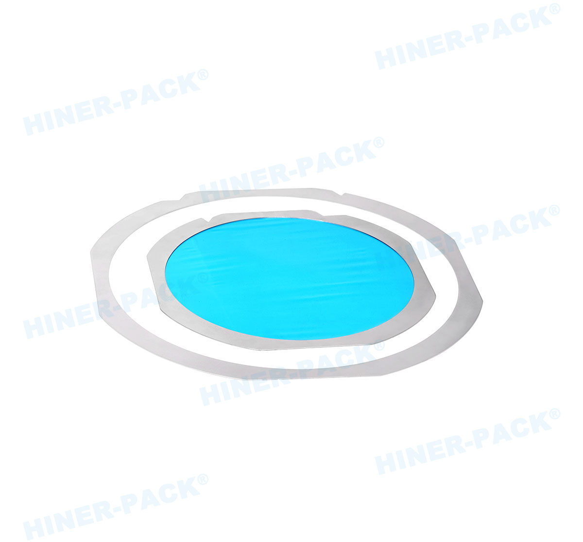
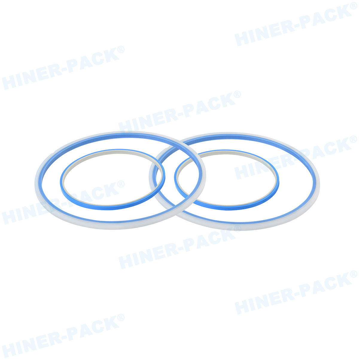
4. Dimensional Accuracy and Automation Interfaces
Carriers must interface with SMIF pods, FOUP load ports, or manual wafer
transfer tools. Critical dimensions include:
Slot pitch (e.g., 4.76 mm for 25‑slot 200mm cassette).
Wafer pocket width and radius – to prevent edge contact.
Kinematic coupling features (three balls or grooves) for repeatable
positioning.
Barcode pocket or RFID well for traceability.
Request a full 2D drawing with GD&T (Geometric Dimensioning and
Tolerancing) and, if possible, a 3D STEP file for virtual simulation with your
automation equipment.
5. Process Validation and Lifecycle Testing
Ask the supplier about their validation protocols:
Mechanical cycling: 10,000+ insert/extract cycles with no
visible wear or particle increase.
Thermal cycling: 200 cycles between -40°C and +125°C with
less than 0.1% dimensional change.
Chemical resistance: Soak in isopropanol, acetone, or SC1
solution for 24 hours – no surface crazing or mass change.
Hiner-pack maintains documented
test data for each carrier family and can share results under NDA.
Types of Wafer Carriers and Supplier Specializations
Different process steps require different carrier designs. A full‑service
wafer carrier
supplier offers multiple families:
Process cassettes (vertical or horizontal): For wet bench,
furnace, or track equipment. Materials: PFA, quartz, or PEEK for high
temperature.
Storage and shipping carriers (single‑wafer or
multi‑wafer): Often polycarbonate or static dissipative ABS with foam
inserts.
FOUP alternatives: For 300mm wafer handling in
semi‑automated lines – carriers with front opening interface and robotic
flanges.
Film frame carriers: For diced wafers mounted on dicing
tape, used in die attach and sorting.
Supplier Audits and Quality Management Systems
Beyond product specifications, evaluate the supplier's manufacturing
environment. Key questions:
Is the injection molding performed in an ISO 7 (Class 10,000) or cleaner
environment?
Does the supplier use automated de‑gating and ultrasonic rinsing to remove
flash and residues?
Are final assemblies double‑bagged in ESD‑shielded bags inside a
cleanroom?
Does the supplier maintain ISO 9001:2015 and IATF 16949 (for automotive
semiconductor carriers)?
A transparent wafer carrier
supplier welcomes customer audits and provides batch records
traceable to raw material certificates.
Custom Engineering Support – When Standard Carriers Are Not Enough
Many applications require modifications: special slot pitch for thin wafers,
cutouts for robot end‑effectors, or integrated RFID holders. A capable supplier
offers:
In‑house mold design and simulation: Moldflow analysis to
minimize warpage and residual stress.
Prototyping via additive manufacturing: Low‑quantity
(<100) functional carriers using antistatic photopolymers for feasibility
tests.
Secondary operations: Laser marking, conductive coating
application, or assembly of foam/gel inserts.
Hiner-pack provides engineering
consultation to translate your wafer handling requirements into a custom carrier
design, with lead times as short as 4 weeks for prototype tooling.
Documentation and Compliance for Regulated Environments
For medical device or automotive semiconductor customers, your wafer carrier
supplier must provide:
Certificate of Conformance (CoC) for each lot, including particle count and
ESD test results.
Material data sheets and safety data sheets (SDS).
SEMI S2 / S8 compliance report for equipment safety and ergonomics.
Conflict minerals declaration (if applicable).
Suppliers unable to provide this documentation create delays during customer
quality audits.
Frequently Asked Questions (FAQs) about Wafer Carrier Supplier
Selection
Q1: What certifications should I look for from a wafer carrier
supplier?
A1: Minimum requirements: ISO 9001:2015 for quality
management. For high‑reliability sectors, look for IATF 16949 (automotive) or
AS9100D (aerospace). Additionally, the supplier should comply with SEMI E15
(carrier interface standards) and provide ISO 14644‑1 cleanroom manufacturing
evidence.
Q2: Can a wafer carrier supplier provide carriers for both 200mm and
300mm wafers?
A2: Yes, many suppliers offer both sizes. However, the
designs differ significantly: 200mm carriers typically use horizontal or
vertical open cassettes, while 300mm often uses FOUP‑style sealed carriers.
Confirm that the wafer carrier
supplier has experience with your specific automation equipment
(e.g., Brooks, Daifuku, or Rorze).
Q3: How long does a typical wafer carrier last in a production fab
environment?
A3: A high‑quality PEEK or PP carrier can withstand 5–7
years of regular use if cleaned properly (ultrasonic bath + DI rinse).
Polycarbonate carriers last 1–3 years, as they become brittle from UV exposure
and solvent residues. The supplier should provide estimated lifecycle data based
on accelerated testing.
Q4: What is the difference between a wafer carrier and a wafer
shipper?
A4: A wafer carrier is typically reusable and designed for
in‑process handling, storage, and automated equipment. A wafer shipper is a
single‑trip or limited‑trip package for transportation between sites. However,
some suppliers use the terms interchangeably. A wafer carrier
supplier often provides both product lines but with different
material grades (carriers require higher purity and durability).
Q5: How do I verify a carrier’s ESD performance before ordering large
volumes?
A5: Request two to five samples from the wafer carrier
supplier and perform your own in‑house tests: surface resistance
(using concentric ring electrodes), discharge time, and charge generation
measurement (using a Faraday cup and electrometer). Also check the carrier’s
performance after three cleaning cycles to ensure the ESD property does not
degrade.
Start Your Supplier Qualification Process Today
Selecting the right wafer carrier
supplier directly affects wafer yield, equipment uptime, and audit
readiness. Hiner-pack combines material
science expertise, precision injection molding, and full documentation to serve
semiconductor fabs and OSATs worldwide. Whether you need standard 25‑slot PEEK
cassettes for wet etching or custom carriers for thin wafer handling, our
engineering team will provide samples, test reports, and a compliance
package.
Request your quotation and validation samples: https://www.waferboxes.com/contact – Include your wafer diameter, process environment (temperature, chemicals), and
automation interface. We will respond with a technical proposal and a supplier
audit checklist within 48 hours.


