
In the high-stakes world of semiconductor manufacturing, the value of a single bare die can range from a few cents to hundreds of dollars. Whether you are handling Indium Phosphide (InP) optical chips or fragile MEMS sensors, the method of transport is often the weakest link in the supply chain. Standard waffle packs allow for movement, which leads to edge chipping. This is where Gel Pak ESD boxes become an indispensable tool for process engineers.
These specialized carriers utilize a proprietary gel material to hold components in place using surface tension rather than mechanical force. However, simply holding the part is not enough. The Electrostatic Discharge (ESD) protection integrated into these boxes ensures that sensitive device architectures are not compromised by static events during handling. For companies sourcing through partners like Hiner-pack, understanding the specific engineering properties of these boxes is key to maintaining high yield.
The Mechanics of Gel Retention
The core technology behind Gel Pak ESD boxes is a cross-linked polymer material. Unlike traditional adhesives, this gel does not rely on chemical bonding to secure the device. Instead, it uses intrinsic surface tension.
When a flat component is placed on the gel, the contact area creates a vacuum-like hold. This prevents the component from sliding laterally or bouncing vertically, even if the box is dropped or inverted.
This "zero-shift" capability is crucial for automated lines. If a pick-and-place machine expects a die at coordinates X,Y, and the die has shifted by 0.5mm during transit, the machine will fail to pick it, or worse, crush it.
The retention level of the gel is customizable. It is typically graded (e.g., extremely low, low, medium, high). A heavy ceramic sub-mount requires high retention, whereas a thinned 50-micron GaAs wafer requires a lighter touch to avoid cracking during removal.
Understanding ESD Properties in Gel Carriers
Static electricity is a constant threat in backend processing. A standard plastic box is an insulator; it can generate and hold a charge. If a technician touches a charged box and then the component, the discharge can vaporize the microscopic traces on the chip.
Gel Pak ESD boxes mitigate this through two primary methods: conductive composites and antistatic coatings.
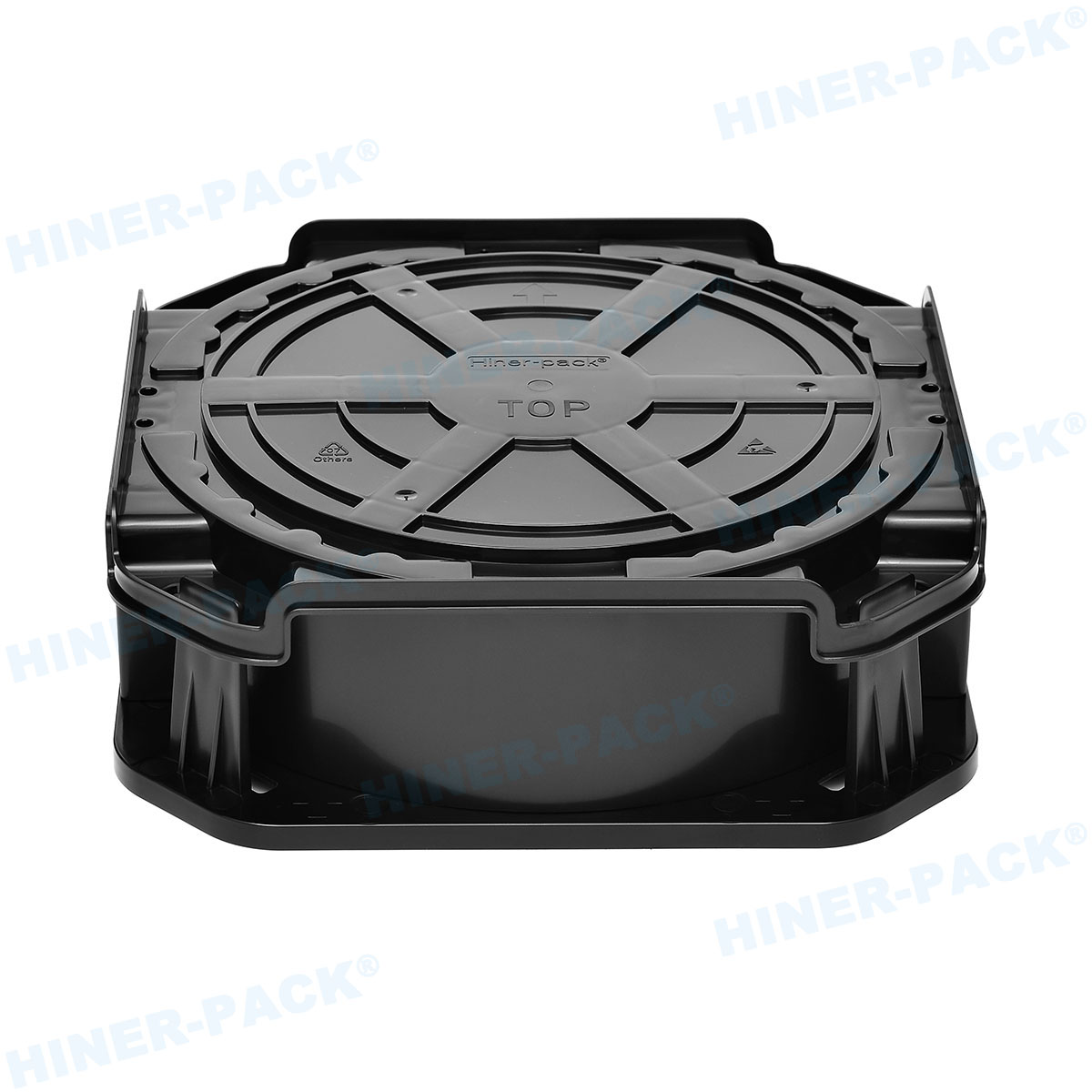
The black boxes are typically conductive. They are molded using carbon-loaded materials that provide a clear path to ground. The surfaceresistance is usually in the range of 10' to 10S ohms. This allows any charge to dissipate instantly when the box is placed on a groundedworkstation.
The clear or transparent boxes often use antistatic or static-dissipative polymers. These are useful when visual inspection is required without opening the box. However, for the most sensitive components, the black conductive format is the industry gold standard.
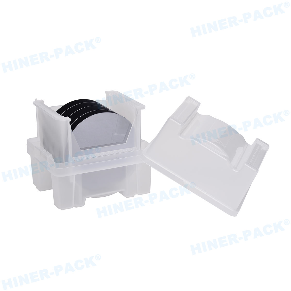
Vacuum Release (VR) Technology
One of the challenges with sticky carriers is getting the part off. If the adhesion is too strong, tweezers can damage the die edges, or vacuum tips can leave residue.
To solve this, many Gel Pak ESD boxes utilize Vacuum Release (VR) technology. In this configuration, the gel membrane is placed over a mesh tray.
During transport, the gel contacts the underside of the component, holding it firm. When it is time to remove the part, the tray is placed on a vacuum fixture. The vacuum pulls the gel membrane down through the mesh holes.
This action reduces the surface area contact between the gel and the component by over 95%. The component is effectively "released" and sits loosely on the mesh texture, allowing for easy removal by automated equipment or hand tools.
The Problem with Standard Waffle Packs
For decades, waffle packs (matrix trays) were the default. They rely on a pocket that is slightly larger than the component.
The issue is the "pocket clearance." To load a component, the pocket must be bigger than the chip. This gap allows the chip to rattle. During international shipping, high-frequency vibrations cause the dies to tumble.
Silicon dust acts as an abrasive. As chips rattle in a waffle pack, they generate particles. These particles can short out active areas on the die surface.
Gel Pak ESD boxes eliminate this movement entirely. By immobilizing the die, particle generation is virtually non-existent. For cleanroom environments classified ISO 5 or better, this reduction in particulate contamination is a significant advantage.
Hiner-pack and Supply Chain Consistency
Sourcing these specialized carriers requires attention to detail. A variation in the gel's "tackiness" or the box's dimensional stability can disrupt a production line.
Hiner-pack has established itself as a reliable node in the semiconductor packaging ecosystem. They understand that a box is not just a container; it is a process tool.
Ensuring that the hinged lids close securely and that the clips (often referred to as "slide clips") engage properly is vital. If a clip fails during transit, the box opens, and thousands of dollars of inventory are lost.
Furthermore, Hiner-pack emphasizes the importance of shelf life. The gel properties can change over years if stored improperly. Fresh stock ensures consistent retention values.
Thermal Stability and Process Integration
Engineers often ask if Gel Pak ESD boxes can withstand heat. The answer depends on the specific series of the box.
Some standard gels are rated for temperatures up to 60°C or 70°C, which is sufficient for shipping. However, some processes require the die to be heated while still in the carrier (e.g., for wire bonding or curing).
High-temperature variants are available that can withstand up to 150°C or even 220°C for short durations. Using the wrong box in a curing oven will cause the gel to reflow, permanently bonding the chips to the carrier.
Before integrating these boxes into a workflow, it is essential to map out the thermal profile the carrier will experience.
Handling Thin and Fragile Wafers
The semiconductor industry is moving toward thinner wafers. Power devices and RF chips are often thinned to 100 microns or less to improve heat dissipation and electrical performance.
A thinned wafer is as fragile as a potato chip. Traditional handling methods usually result in breakage.
Gel Pak ESD boxes provide a uniform support structure. Because the entire backside of the die is supported by gel, there are no pressure points.
When using VR (Vacuum Release) trays, the vacuum must be applied slowly. A sudden snap of the vacuum can flex the thin die. Modern VR fixtures allow for ramped vacuum pressure to gently release these delicate components.
Cleaning and Reusability
While many packaging materials are single-use, the cost of high-end gel carriers often dictates that they be reused, especially in internal factory logistics.
The gel surface can accumulate dust over time, which reduces tackiness. If the tackiness drops, the risk of component shift increases.
Cleaning Gel Pak ESD boxes is possible but requires strict protocols. Using transparent tape (like Kapton or Scotch tape) to lift debris off the gel is a common method. Liquid cleaning is riskier, as certain solvents can degrade the gel chemistry or the ESD properties of the box casing.
Most manufacturers recommend a "dry clean" approach using adhesive rollers specifically designed for this purpose.
Logistics and Exterior Packaging
Even with the best gel box, the exterior packaging matters. The box protects the die; the shipping carton protects the box.
When shipping Gel Pak ESD boxes, they should be packed in shielded bags to create a Faraday cage effect. This adds a second layer of ESD protection.
Bubble wrap or foam should be used to prevent the plastic boxes from cracking if the parcel is crushed. Hiner-pack advises using rigid outer cartons rather than padded envelopes, as the hinges on the plastic boxes can snap under crushing loads.
Labeling is also critical. Labels should indicate "Fragile" and "ESD Sensitive" to ensure handlers are aware of the contents' nature.
The transition from standard mechanical packaging to gel-based solutions marks a maturity in a manufacturing process. When yield loss due to transit damage becomes unacceptable, Gel Pak ESD boxes offer the necessary security.
They bridge the gap between the fabrication plant and the assembly house. By combining static dissipation with mechanical immobilization, they solve two of the biggest threats to semiconductor devices simultaneously.
Whether you are a startup lab or a high-volume foundry, the choice of carrier affects your bottom line. Partnering with experienced suppliers like Hiner-pack ensures that you have access to the right configuration—be it vacuum release, conductive, or high-temp—to keep your chips safe and your customers happy.
Frequently Asked Questions (FAQ)
Q1: What is the shelf life of Gel Pak ESD boxes before the gel loses its stickiness?
A1: Generally, the shelf life is two years from the date of manufacture if stored in a cool, dry environment away from direct sunlight. Over time, the gel may slightly change in tackiness, but the ESD properties of the box material typically remain stable for much longer.
Q2: Can I use liquid solvents to clean the gel surface?
A2: It is generally not recommended to use alcohol or harsh solvents on the gel, as they can absorb into the polymer and alter its retention force. The best method for cleaning is using a low-tack adhesive tape to lift off dust and particles without leaving a residue.
Q3: How do I choose between standard gel boxes and Vacuum Release (VR) boxes?
A3: Standard gel boxes are suitable for robust components that can be picked up with tweezers or by hand. Vacuum Release (VR) boxes are essential for very fragile, thinned, or large-area devices where the force required to pull them off the gel would cause cracking or damage.
Q4: Are the black Gel Pak ESD boxes better than the clear ones?
A4: For ESD protection, yes. Black boxes are typically conductive (carbon-loaded) and offer the fastest charge dissipation. Clear boxes are usually anti-static or static-dissipative. While clear boxes allow for visual inspection, black boxes provide a more robust shield against static damage for highly sensitive components.
Q5: Will the gel leave a residue on the back of my optical devices?
A5: High-quality Gel Pak ESD boxes use a cross-linked polymer that is designed to be non-outgassing and non-transferring. In most semiconductor applications, they are considered "residue-free." However, for extremely sensitive surface science applications, it is always best to perform a validation test with your specific device material.


