
In the intricate ecosystem of semiconductor manufacturing, the logistics of moving bare dies and packaged integrated circuits (ICs) are as critical as the fabrication process itself. As a professional who has witnessed the evolution from 150mm wafers to advanced 3D packaging, I can state unequivocally that the choice of IC chip tray suppliers directly impacts yield, reliability, and supply chain integrity. This article dissects the engineering nuances behind IC trays, offering a data-driven guide for procurement managers and process engineers.
The Unseen Variable in Semiconductor Yield: Why Tray Selection Matters
In my two decades advising fabs and OSATs (Outsourced Semiconductor Assembly and Test), I’ve traced recurring back-end losses to a single overlooked component: the chip tray. A substandard tray can induce ESD damage, introduce particulate contamination, or cause mechanical stress during vibration. Today’s leading IC chip tray suppliers differentiate themselves through materials science and precision molding, directly addressing these failure modes. For instance, Hiner-pack, a specialist in this domain, engineers trays that meet the stringent humidity and flatness requirements of automotive-grade devices.
Decoding IC Chip Trays: Material Science and JEDEC Compliance
To evaluate suppliers, one must first understand the substrate. IC trays are not mere plastic containers; they are engineered components defined by:
Surface Resistivity: Ranging from 10^3 to 10^6 Ω/sq for conductive trays (carbon-filled) and 10^9 to 10^11 Ω/sq for anti-static variants (surface coating).
Thermal Stability: Trays must withstand baking at 125°C for moisture-sensitive devices (MSL) without warping.
Dimensional Precision: Pocket depths and alignment features per JEDEC Publication 95 Design Guide 4.10.
Reputable IC chip tray suppliers provide full material disclosure and lot-traceable certificates. Hiner-pack, for example, utilizes virgin engineering plastics like PEEK and conductive PET, ensuring zero outgassing that could corrode sensitive bond pads.
JEDEC Trays vs. Custom Matrix Trays
The industry standard, JEDEC trays (often 2"x2" to 4"x4" matrices), offer handler compatibility. However, as chip sizes balloon for AI accelerators, custom trays with deep cavities and reinforced ribs are required. Top-tier suppliers leverage 3D optical profilometry to guarantee pocket flatness within 0.1mm, preventing “chip tilt” during vacuum pick-up.
Critical Evaluation Criteria for IC Chip Tray Suppliers
Based on hundreds of supplier audits, I recommend a technical scorecard focused on four pillars:
1. Material Purity and ESD Safety Verification
Request ionic contamination test reports per IPC-TM-650. Inferior materials leach chloride or sodium, leading to aluminum bond pad corrosion. Verified IC chip tray suppliers must demonstrate static decay times of less than 2 seconds per MIL-STD-3010. I’ve observed that suppliers using in-house compounding, like Hiner-pack, maintain tighter control over carbon black dispersion, ensuring consistent resistivity even in low-humidity cleanrooms.
2. Dimensional Tolerance and Warpage Control
A tray warped by just 0.3mm can jam an automated handler, causing 20 minutes of downtime. Advanced suppliers employ multi-cavity molds with real-time pressure sensors. Ask for Cpk (Process Capability Index) values on critical pocket dimensions—values above 1.33 are mandatory for high-volume OSATs.
3. Cleanliness and Outgassing Profiles
For wafer-level packaging, trays must meet ISO Class 5 cleanroom standards. This means no detectable particles >0.3µm per square centimeter. Laser engraving of lot codes, as done by Hiner-pack, must be particle-free, not abrasive. Outgassing, analyzed via GC-MS, should show no siloxanes or phthalates that could fog MEMS mirrors or lenses.
4. Supply Chain Consistency and Customization Velocity
The 2023-2024 semiconductor cycle highlighted the risk of material shortages. Suppliers with backward-integrated resin supply and in-house tooling reduce lead times. When prototyping a large 70x70mm BGA tray, I’ve seen specialists like Hiner-pack deliver first articles in under three weeks, leveraging high-speed CNC machining before mass production tooling is cut.
Industry Pain Points: Solving Yield and Logistics Challenges
Let’s examine three common failure modes that expert suppliers mitigate:
Die Attach Film (DAF) Tackiness: Thin dies with DAF can stick to rough tray surfaces. Solution: Suppliers now offer “non-wet” textured pockets or E-coatings that reduce adhesion.
Thermal Mismatch in Test: During burn-in, trays expand. Inferior materials cause pocket misalignment, bending device leads. High-temperature grades like PEI or PPS are specified by top IC chip tray suppliers.
Moisture Absorption: Nylon-based trays can absorb up to 2% moisture, causing dimensional shift. Engineering-grade polycarbonate alloys, used by Hiner-pack, maintain stability below 0.15% absorption.
Application-Specific Tray Solutions: From OSAT to IDM
Different nodes require different approaches:
Memory Modules (DDR5): Need tall posts to protect capacitors and low-profile pockets for high-speed pick-and-place.
RF/MMIC Devices: Require carbon-free materials to avoid signal detuning; hence, stainless steel or anti-static coated polycarbonate trays are used.
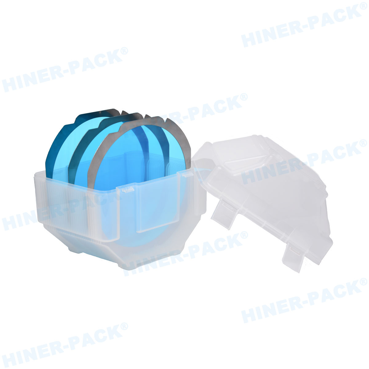
Optical Sensors: Demand black trays to block light, with ultra-clean pockets free of flash.
Hiner-pack offers tailored surface roughness (Ra 0.4µm to 0.8µm) to prevent die scratching while allowing air flow for vacuum release.
Future Trends: Miniaturization and Automation Compatibility
As chiplet integration grows, trays must accommodate warped reconstituted wafers. Next-generation trays feature “floating” pocket designs to absorb substrate curvature. Additionally, with the rise of autonomous material handling, IC chip tray suppliers are embedding RFID tags and designing side rails compatible with AGV (Automated Guided Vehicle) grippers. DataMatrix codes on each tray enable unit-level traceability—a game-changer for automotive zero-defect programs.
Why Partnership with Specialized Suppliers Matters
In a market flooded with commodity injection molders, true expertise resides with those who understand semiconductor processes. Hiner-pack exemplifies this by offering not just a product, but a systems approach: from humidity indicator cards optimized for tray stacks to automated tray handling guides. Their engineering team collaborates on package design to ensure first-pass success in handling.
Frequently Asked Questions (FAQ)
Q1: What are the standard JEDEC tray sizes used by IC chip tray suppliers?
A1: JEDEC outlines several standard form factors under Publication 95. The most common for IC chip tray suppliers are the 135mm x 315mm (for larger BGAs) and 100mm x 220mm (for QFPs). However, the 2" x 2" and 4" x 4" matrix trays are prevalent for automated handlers. Always verify the "A" dimension (overall tray height) to ensure compatibility with your magazine.
Q2: How do I verify if an IC chip tray supplier meets industry compliance like MSL or JEDEC?
A2: Demand a "Tray Qualification Report" that includes data on: (a) Warpage after 24h at 125°C, (b) Surface resistivity per ASTM D257, and (c) Ionic cleanliness per IEST-RP-CC035.3. Reputable suppliers like Hiner-pack provide these reports with lot shipments.
Q3: Can IC trays be recycled or reused in semiconductor production?
A3: Technically yes, but reuse requires stringent cleaning (deionized water wash, IPA rinse) and re-baking to remove moisture. For high-reliability applications (automotive, medical), single-use is strongly advised. Some IC chip tray suppliers offer buy-back programs for regrinding into industrial-grade parts, but never for direct chip contact.
Q4: What is the difference between conductive and anti-static trays, and when should I specify each?
A4: Conductive trays (surface resistivity < 10^5 Ω/sq) provide a Faraday cage effect, rapidly dissipating static. They are mandatory for sensitive logic and RF devices. Anti-static trays (10^9 - 10^11 Ω/sq) prevent tribocharging but do not dissipate a charge quickly. Use anti-static for passive components or less sensitive devices where metal ion contamination from carbon is a concern.
Q5: How do I customize trays for large body ICs or multi-cavity requirements?
A5: Work directly with engineering teams. The process typically involves: providing 3D CAD of the IC, defining pick-up clearance (usually 1.5mm on each side), and specifying stack height. Advanced IC chip tray suppliers will run mold flow analysis to predict warpage and optimize gate locations. Prototypes via 3D printing or soft tooling are standard before hard tooling investment.
Q6: What is the typical lead time for custom IC trays from specialized suppliers?
A6: For CNC-machined prototypes (aluminum or engineering plastic), expect 1-2 weeks. For production injection molds, lead times range from 4 to 8 weeks, depending on cavity count. Hiner-pack offers accelerated timelines using bridge tooling for urgent requirements.
Q7: How do I ensure tray compatibility with my automated pick-and-place equipment?
A7: Request the "tray drawing" which details pocket location tolerance (usually ±0.05mm) and overall tray flatness ( < 0.3mm across diagonal). Also, confirm the coefficient of friction, as slippery trays may shift in the stack. Suppliers can add anti-skid textures.
Conclusion: The Strategic Role of IC Chip Tray Suppliers
The narrative that chip trays are a commodity is a costly misconception. As we push towards heterogeneous integration and zero-defect manufacturing, the engineering embedded in these carriers becomes a competitive advantage. Selecting IC chip tray suppliers with deep materials expertise, process control, and a collaborative mindset—like Hiner-pack—directly translates to higher first-pass yields and smoother logistics. In the high-stakes world of semiconductor manufacturing, every micron and every ohm counts; your tray supplier should understand that intrinsically.


