
1. Why reusable wafer trays reduce long-term operating costs
Single-use packaging generates constant reordering and waste disposal fees. Reusable wafer trays are moulded from durable polymers that endure hundreds of trips. Facilities that switch to reusables typically see ROI within 12 to 18 months.
Lower per-cycle cost compared to disposable alternatives.
Reduced inventory management overhead.
Minimised waste disposal expenses and environmental fees.
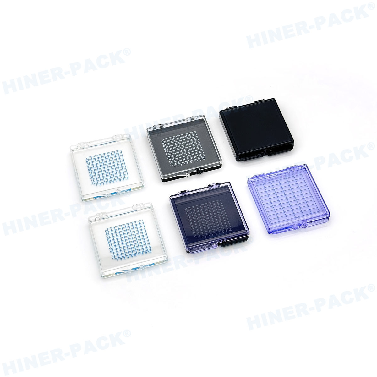
1.1 Material durability for repeated use
High-performance PES, PEEK, or conductive PP withstand autoclave and DI water cleaning.
Dimensional stability after hundreds of thermal cycles.
Resistance to chemicals like IPA and NMP used in wafer fabs.
2. Environmental impact and sustainability goals
Semiconductor companies are under pressure to reduce packaging waste. Hiner-pack supports these initiatives by supplying reusable wafer trays that replace cardboard and single-use plastics. Each reusable tray can eliminate thousands of disposable units over its lifespan.
Less plastic waste sent to landfills or incineration.
Lower carbon footprint from reduced manufacturing and transport of disposables.
Contribution toward corporate ESG (Environmental, Social, Governance) targets.
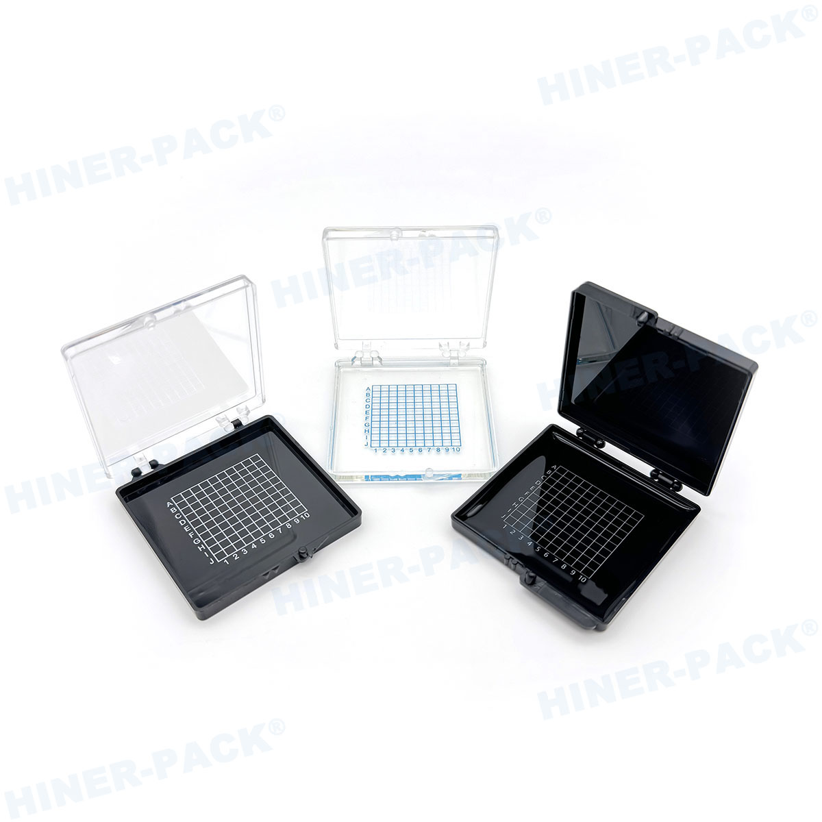
3. Cleanroom compatibility and contamination control
Reusability does not compromise cleanliness. Modern reusable wafer trays are moulded in ISO Class 4 or 5 cleanrooms and packaged in double bags. After each use, they can be cleaned to meet the same stringent standards as new trays.
Materials tested for low outgassing and ionic residues per SEMI standards.
Smooth surfaces with no fissures that could trap particles.
ESD-safe formulations (conductive or dissipative) prevent static damage.
4. Standardisation and equipment compatibility
Reusable wafer trays follow industry-standard form factors (2-inch to 12-inch) to fit existing wafer carriers, FOUPs, and shipping boxes. This ensures seamless integration into automated handling systems without modifying equipment.
Compatible with SEMI M1.15 specifications for wafer shippers.
Stacking features for secure transport in magazines or cassettes.
Alignment features for robotic pick-and-place accuracy.
When you order reusable wafer trays from Hiner-pack, you receive documentation of dimensional conformance to your handling tools.
5. Logistical advantages: returnable program management
Many fabs implement closed-loop systems where empty trays are collected, cleaned, and returned to the wafer supplier. Durable reusable wafer trays simplify these logistics because they withstand repeated shipping without cracking or warping.
Standardised barcode or RFID slots for tracking tray inventory.
Nestable designs to minimise return freight volume.
Long lifespan reduces the frequency of replacement orders.
6. Customisation for specialised wafer types
Thinned wafers, compound semiconductors (GaAs, SiC), and MEMS devices often require specific pocket geometries. Reusable wafer trays can be custom-moulded with features such as:
Deeper cavities for wafers with backside coatings or bumps.
Support ribs that prevent wafer sagging during transport.
Indices for easy identification of wafer orientation.
Hiner-pack offers engineering support to design trays that protect delicate substrates through hundreds of process cycles.
7. Quality assurance and certification for reusable trays
Buyers must verify that reusable wafer trays maintain performance over time. Responsible suppliers provide:
Lot traceability for each moulding run.
Certificates of analysis for cleanliness and ESD properties.
Accelerated aging test data to predict useful life.
When sourcing from Hiner-pack, you receive full material disclosure and recommended cleaning procedures to maximise tray longevity.
In conclusion, reusable wafer trays represent a smart investment for wafer fabs, OSATs, and material suppliers. They cut costs, support sustainability, and maintain the rigorous cleanliness required in semiconductor processing. By choosing a trusted manufacturer like Hiner-pack, you ensure that every tray delivers consistent protection cycle after cycle.
Frequently Asked Questions (FAQ)
Q1: How many times can a reusable wafer tray typically be used?
A1: Depending on the material and cleaning method, high-quality trays can be reused 50 to 200 times or more. Trays made from PES or PEEK often have the longest service life in demanding fab environments.
Q2: What cleaning methods are recommended for reusable wafer trays?
A2: Common methods include ultrasonic cleaning with deionised water and mild surfactants, rinsing with isopropyl alcohol, or automated dishwasher systems designed for cleanroom carriers. Always verify that the cleaning chemistry does not degrade the ESD properties.
Q3: Are reusable wafer trays compatible with all wafer sizes?
A3: Yes, they are available for 2-inch up to 12-inch wafers. Custom inserts or pocket modifications can accommodate thin or warped wafers that do not lie perfectly flat.
Q4: Do reusable trays cost more initially than single-use trays?
A4: The upfront cost is higher, but the cost per use becomes significantly lower after several cycles. Most fabs achieve full payback within one to two years, depending on usage frequency.
Q5: How do I ensure that reused trays still meet cleanroom particle specs?
A5: Implement a periodic inspection and requalification protocol. This can include particle fallout tests, surface resistivity measurements, and visual inspection under UV light. Suppliers like Hiner-pack can provide guidelines for requalification intervals.
Q6: Can reusable wafer trays be recycled at the end of their life?
A6: Yes, most engineering thermoplastics used in these trays (PP, PES, PEEK) are recyclable. Check with your local recycler or the manufacturer for take-back programs that reclaim the material for secondary applications.


