
The photolithography process is a cornerstone of semiconductor manufacturing. It involves transferring intricate patterns onto silicon wafers. A key component in this process is the wafer box for photolithography. This specialized container ensures wafers are protected during handling, storage, and transport.
Without proper protection, wafers can suffer from contamination or damage. This leads to yield loss and increased costs. The wafer box for photolithography addresses these risks. It provides a controlled environment to maintain wafer integrity.
This article delves into the importance, types, and best practices for using wafer boxes. We will also highlight innovations from Hiner-pack, a trusted brand in semiconductor packaging solutions.
The Critical Role of Wafer Box in Photolithography
In photolithography, precision is paramount. Even minor defects can ruin entire batches. The wafer box for photolithography plays a vital role in safeguarding wafers.
Protection from Contamination
Contaminants like dust, particles, or chemical residues can disrupt lithography patterns. A wafer box for photolithography is designed to minimize exposure. It features sealed compartments and cleanroom-compatible materials.
Key benefits include:
Reduction of airborne particles during storage.
Shielding from environmental humidity and static.
Compatibility with cleanroom protocols for photolithography.
Mechanical Stability and Handling
Wafers are fragile and require careful handling. The wafer box for photolithography provides structural support. It prevents bending, cracking, or scratching during automated or manual processes.
Design features often include:
Secure slots to hold wafers in place.
Ergonomic handles for safe transport.
Stackable designs for efficient storage.
Types of Wafer Boxes for Photolithography
Different photolithography stages require specific wafer box designs. Selecting the right type is crucial for operational efficiency.
Standard Wafer Boxes
These are commonly used for general storage and transport. They are made from materials like polypropylene or polycarbonate. Standard boxes offer basic protection and are cost-effective for bulk handling.
Typical applications:
Interim storage between photolithography steps.
Transport within fabrication facilities.
Compatibility with standard wafer sizes like 200mm or 300mm.
Advanced Wafer Boxes
For high-end photolithography, advanced boxes provide enhanced features. They may include anti-static properties, RFID tagging, or climate control. These boxes support advanced nodes and sensitive processes.
Features to consider:
Low-outgassing materials to prevent chemical contamination.
Integrated sensors for monitoring temperature and humidity.
Customizable layouts for specialized wafer configurations.
Selecting the Right Wafer Box for Photolithography
Choosing a wafer box for photolithography involves several factors. It impacts yield, cost, and workflow efficiency.
Material Considerations
Materials must meet cleanroom standards. They should be non-shedding and chemically inert. Common choices include:
Polycarbonate for durability and clarity.
PEEK for high-temperature resistance.
Anti-static polymers to reduce electrostatic discharge.
Size and Capacity
Wafer boxes come in various sizes to match wafer diameters. Capacity refers to the number of wafers per box. Balancing space and protection is key.
Guidelines:
Ensure compatibility with photolithography equipment load ports.
Opt for modular designs that allow scalability.
Consider footprint for storage in limited cleanroom spaces.
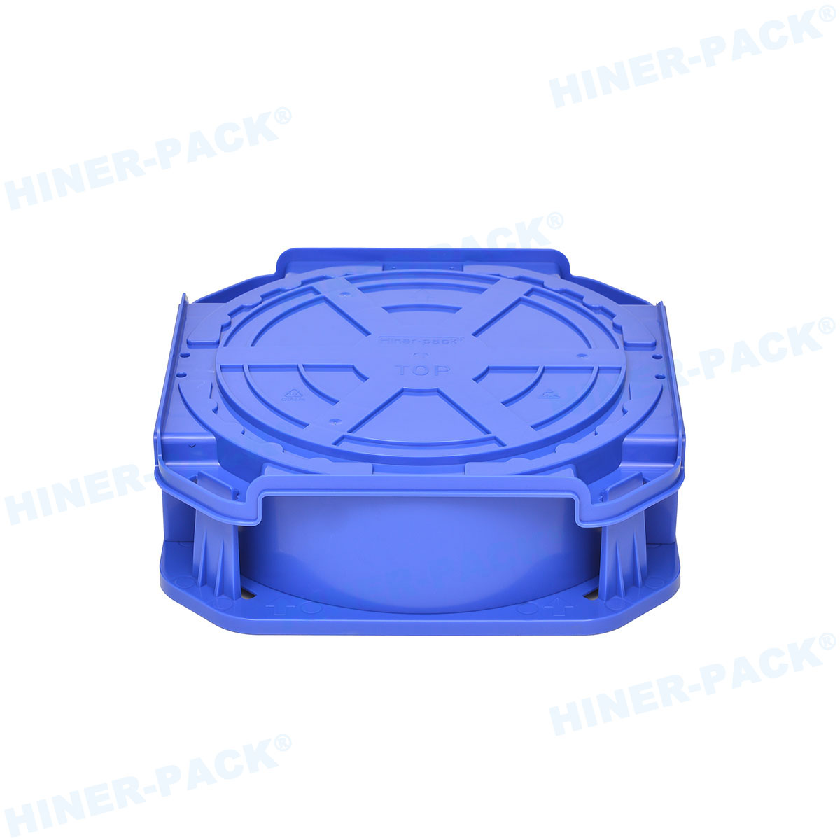
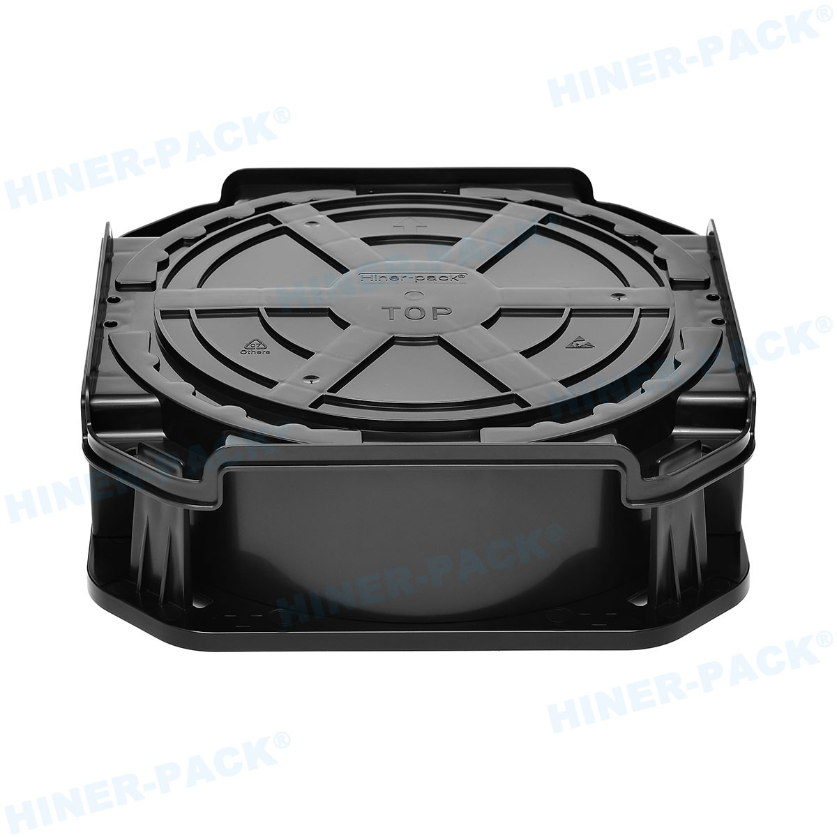
Hiner-pack's Innovations in Wafer Box for Photolithography
Hiner-pack is a leading provider of semiconductor packaging solutions. Their wafer box for photolithography is designed for reliability and performance.
Product Features
Hiner-pack boxes incorporate advanced engineering. They focus on minimizing contamination and maximizing durability.
Notable features:
Proprietary materials that reduce particle generation.
Precision-molded slots to prevent wafer movement.
Compliance with SEMI standards for photolithography applications.
Quality Assurance
Hiner-pack implements rigorous testing protocols. Each wafer box for photolithography undergoes inspections for defects and performance.
Quality measures include:
Cleanroom certification to ISO Class 1 levels.
Stress testing under simulated photolithography conditions.
Traceability systems for batch tracking and recall management.
Best Practices for Using Wafer Box in Photolithography
Proper usage extends the life of wafer boxes and protects wafers. Follow these guidelines for optimal results.
Handling and Storage
Always handle wafer boxes with clean gloves. Store them in controlled environments to avoid environmental shifts.
Recommendations:
Keep boxes closed when not in use to limit exposure.
Stack boxes evenly to prevent distortion.
Use automated handlers to reduce human error.
Cleaning Procedures
Regular cleaning maintains box integrity. Use approved solvents and methods to avoid material degradation.
Steps for cleaning:
Wipe surfaces with lint-free cloths and isopropyl alcohol.
Inspect for cracks or wear after each cleaning cycle.
Document cleaning schedules to ensure consistency.
Future Trends in Wafer Box Technology for Photolithography
As semiconductor technology advances, wafer box designs evolve. Trends focus on smarter, more integrated solutions.
Emerging developments include:
IoT-enabled boxes with real-time monitoring capabilities.
Sustainable materials to reduce environmental impact.
Custom designs for next-generation photolithography tools.
These innovations will further enhance the role of wafer box for photolithography in manufacturing.
Conclusion
The wafer box for photolithography is a fundamental tool in semiconductor fabrication. It ensures wafers remain pristine from storage to processing. Selecting the right box involves careful consideration of materials, size, and features.
Brands like Hiner-pack drive progress with reliable and innovative solutions. By following best practices, manufacturers can optimize yield and reduce costs. The future of wafer box for photolithography looks promising with ongoing technological advances.
Frequently Asked Questions (FAQ)
Q1: What is the primary function of a wafer box for photolithography?
A1: The primary function is to protect silicon wafers from contamination, mechanical damage, and environmental factors during handling, storage, and transport in photolithography processes. It helps maintain wafer integrity and improve yield.
Q2: How do I choose the right material for a wafer box in photolithography?
A2: Select materials based on cleanroom compatibility, chemical resistance, and durability. Common options include polycarbonate for clarity and PEEK for high-temperature applications. Always check compliance with industry standards like SEMI.
Q3: Can wafer boxes be reused in photolithography, and how should they be cleaned?
A3: Yes, many wafer boxes are reusable. Clean them regularly using lint-free cloths and approved solvents like isopropyl alcohol. Inspect for damage after cleaning to ensure continued protection.
Q4: What are the key features of Hiner-pack's wafer box for photolithography?
A4: Hiner-pack's boxes feature low-particle materials, precision molding for secure wafer placement, and compliance with SEMI standards. They also include quality assurance measures like cleanroom certification and traceability systems.
Q5: How does wafer box design impact photolithography efficiency?
A5: Design impacts efficiency by ensuring compatibility with equipment, reducing contamination risks, and enabling smooth handling. Well-designed boxes minimize downtime and support automated workflows in photolithography.


