In the high-stakes environment of semiconductor fabrication and backend
assembly, the carriers that transport, store, and protect critical substrates
are not merely passive packaging components. They are active contributors to
yield, cleanliness, and process stability. Semiconductor tray standards represent the
convergence of mechanical tolerances, material science, electrostatic discharge
(ESD) control, and automated handling requirements. For process engineers,
quality managers, and supply chain specialists, deviating from established
specifications introduces risks ranging from micro-contamination to robotic
pick-and-place failures—each capable of eroding profitability in high-volume
manufacturing (HVM).
This analysis dissects the core pillars of modern semiconductor tray
standards, aligning them with industry roadmaps, equipment interfaces
(such as SEMI and JEDEC), and emerging requirements for advanced packaging. We
will explore how standardized dimensions, tailored material formulations, and
rigorous cleanliness protocols form the foundation of reliable wafer logistics.
Companies such as Hiner-pack have operationalized these standards to
deliver precision carriers that bridge the gap between front-end fabs and
back-end assembly lines.
1. The Structural Pillars of Semiconductor Tray Standards
The landscape of wafer and substrate carriers is defined by a hierarchy of
standards that govern geometry, material properties, and performance under
real-world fab conditions. Unlike generic industrial trays,
semiconductor-specific carriers must satisfy multiple, often conflicting,
requirements: ultra-low particle generation, dimensional stability across
temperature variations, static dissipation, and compatibility with automated
material handling systems (AMHS).
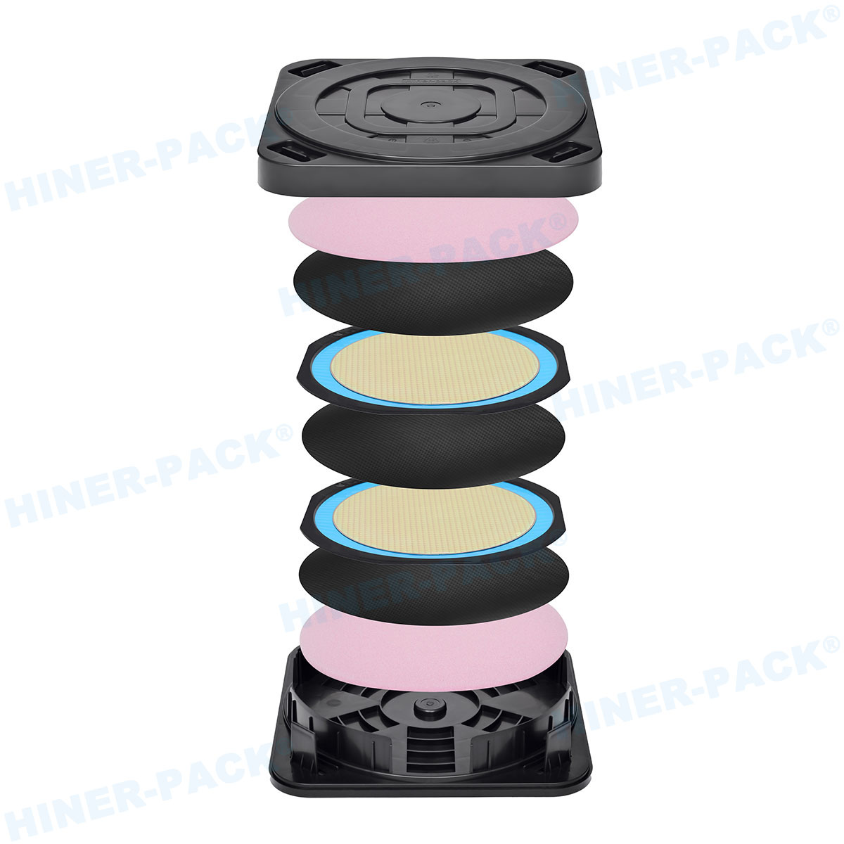
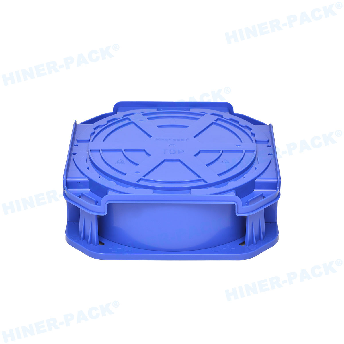
1.1 Dimensional Specifications and Tray Stacking
At the heart of semiconductor tray standards lies
dimensional interoperability. Tray formats must align with SEMI E1.9
(specifications for plastic wafer shipping trays) and JEDEC design outlines for
matrix trays used in assembly. Key parameters include pocket depth, chamfer
angles, and rib structures that prevent wafer edge contact while ensuring
nestling during thermal cycling. For 300mm wafers, trays must accommodate not
only the substrate diameter but also the variations from wafer bow and
warp—critical for thin wafers used in 3D integration.
Stacking compatibility is equally vital. Interlocking features, alignment
pins, and uniform stack heights allow automated de-nesting systems to operate
without jamming. Standardized stacking pitch (often 12.7mm or 19.05mm per tray)
ensures that magazine loaders and stockers function predictably across different
suppliers. When trays deviate from these norms, the risk of tool stoppages
increases, translating to downtime measured in thousands of dollars per hour in
a high-volume fab.
1.2 Material Selection and Contamination Control
Material science directly dictates whether a tray meets cleanroom
compatibility standards. Polycarbonate (PC), polyethylene terephthalate glycol
(PETG), and polyetheretherketone (PEEK) are prevalent, each offering distinct
trade-offs between rigidity, ESD performance, and outgassing. For advanced nodes
(sub-7nm), ionic contamination and volatile organic compounds (VOCs) from trays
can cause gate oxide defects or photoresist poisoning. Therefore, strict
adherence to semiconductor tray standards mandates maximum
allowable levels of extractable ions (fluorine, chlorine, sodium) as per SEMI
C3.2 and ASTM E595 for outgassing.
Industry-leading manufacturers employ injection molding under ISO 14644-1
Class 7 or cleaner environments, followed by ultrasonic cleaning and
vacuum-sealed packaging. Hiner-pack, for instance, integrates these
cleanliness protocols into their production workflow, ensuring that trays meet
the stringent particle specifications (e.g., < 50 particles ≥0.3 µm per tray)
required by leading IDMs and OSATs.
2. ESD Control and Surface Resistivity Standards
Electrostatic discharge remains a persistent threat in semiconductor
handling, with device sensitivities extending to below 20V for some RF and
memory components. Semiconductor tray standards categorize
materials based on surface resistivity ranges: conductive (< 1E5 ohms/sq),
static dissipative (1E5 to 1E12 ohms/sq), and anti-static (> 1E12 ohms/sq
with static decay < 2 seconds). The choice depends on application: conductive
materials may risk shorting device leads, while insulative materials allow
charge accumulation that leads to field-induced damage.
Industry consensus, reflected in ANSI/ESD S20.20 and SEMI E129, favors
static-dissipative materials for wafer trays, often achieved through
carbon-loading or inherently dissipative polymers. The challenge lies in
balancing dissipation with particle cleanliness—carbon-fiber filled compounds
can generate loose particulates unless encapsulated by advanced compounding
techniques. Modern specifications require that after 10,000 cycles of automated
handling, a tray’s ESD properties remain stable and its particulate generation
remains within Class 1 cleanroom limits.
3. Advanced Packaging and Customization: Beyond JEDEC Baseline
While baseline semiconductor tray standards provide a
universal foundation, the proliferation of advanced packaging—chiplet
integration, fan-out wafer-level packaging (FOWLP), and hybrid bonding—demands
bespoke tray configurations. Standard JEDEC outlines often fail to accommodate
irregular substrate sizes, singulated dies with non-standard footprints, or
warped reconstituted wafers. Here, the concept of “application-specific trays”
emerges, where pocket geometry, fiducial markers for vision systems, and
material hardness are tailored to unique process flows.
For instance, in FOWLP, reconstituted wafers can measure up to 610mm in panel
form, requiring trays that support panel edges without inducing stress.
Similarly, for thin die (≤100 µm), trays must feature ultra-soft contact
surfaces—often using silicone or elastomeric inserts—to prevent backside
scratching or die breakage during singulation-to-tape-and-reel transfer.
Semiconductor tray standards are thus evolving from
rigid codifications to flexible frameworks that incorporate design for
manufacturability (DFM) agreements between tray suppliers and device
manufacturers.
3.1 Thermal and Chemical Resilience for Harsh Processes
Beyond cleanroom storage, trays are increasingly exposed to elevated
temperatures (e.g., pre-conditioning up to 260°C for lead-free reflow
simulation) and chemical environments (solvents, plasma cleaning residues).
Standard polycarbonate trays cannot withstand such extremes without warping or
outgassing. High-temperature materials like PEEK, Torlon, or ceramic-coated
composites are specified per customer-specific protocols. These high-end trays
must conform to the same external dimensions as standard trays to ensure tool
compatibility, while offering glass-transition temperatures (Tg) above
260°C.
4. Industry Pain Points and Solutions Through Standardization
Despite mature specifications, the semiconductor supply chain continues to
encounter recurring issues related to tray performance. A data-driven approach
reveals three major pain points where adherence to or deviation from
semiconductor tray standards directly impacts yield and
operational efficiency.
Pain Point 1: Tray Warpage During Bake-Out Cycles
Many
assembly houses perform pre-mold or post-mold cure processes that subject trays
to 150–200°C. Trays not qualified to thermal stability standards (e.g., less
than 0.5 mm bow after thermal cycling) can lead to wafer/die slippage,
misalignment during pick-and-place, and tool jams. Solution: Specifying trays
with certified thermal history data and using cross-linked polymers or
metal-reinforced frames.
Pain Point 2: Inconsistent Pocket Dimensions Affecting Automation
Yield
Automated die attach systems and pick-and-place tools rely on
tight pocket tolerances (±0.05 mm). When trays from multiple suppliers exhibit
cumulative tolerances, vision system errors increase. Solution: Adopting
statistical process control (SPC) in tray manufacturing, with 100% optical
inspection of pocket geometry, as practiced by specialized suppliers like
Hiner-pack.
Pain Point 3: Cross-Contamination from Reusable Trays
In
high-mix facilities, trays reused across different product families can
cross-contaminate with flux residues, epoxy bleed-out, or metal particles.
Solution: Implementing RFID-enabled tray tracking combined with validated
cleaning procedures per SEMI E154 (specification for cleaning and packaging of
shipping trays).
5. The Role of Automation and Industry 4.0 Integration
As fabs transition to lights-out manufacturing, semiconductor tray
standards must integrate with digital traceability and robotic
interfaces. Machine-readable features—such as data matrix codes laser-marked
onto tray flanges—are becoming mandatory. These codes link to a centralized
manufacturing execution system (MES) that tracks tray history: number of usage
cycles, cleaning dates, and qualification status. Moreover, standards like SEMI
E142 (specification for identification of shipping trays) define the format and
placement of such codes to ensure readability by overhead hoist transport (OHT)
systems and stockers.
Additionally, standardized notch or flat alignment features ensure that
orientation-dependent devices (e.g., wafers with notches or dies with pin-1
markers) are consistently presented to robotic end effectors. When these
features align with global semiconductor tray standards,
changeovers between different product SKUs can be executed without mechanical
reconfiguration, reducing setup time by up to 30% in backend assembly lines.
6. Compliance and Certification: Navigating Global Specifications
Compliance with semiconductor tray standards is not merely a
technical exercise but a prerequisite for supplier qualification. Leading
semiconductor manufacturers require full documentation covering:
Material Certificates of Analysis (CoA) per SEMI C3 (standards for materials
used in semiconductor processing).
Outgassing test reports per SEMI E108 (standard for outgassing of wafer
shipping trays) or ASTM E595.
ESD verification reports according to ANSI/ESD STM11.11 and STM11.12.
Cleanliness data including particle counts and extractable ions (SEMI C3.2,
C3.3).
Dimensional validation reports using coordinate measuring machine (CMM)
data.
Suppliers such as Hiner-pack maintain these certifications and provide
transparent documentation to streamline the customer qualification process,
reducing the risk of production disruptions due to non-compliant carriers.
7. Future Outlook: Toward Ultra-Low Particle and Recyclable Standards
The next frontier for semiconductor tray standards involves
two seemingly contradictory drivers: lower allowable particle limits
(approaching 0.1 µm detection thresholds for leading-edge logic) and
sustainability mandates for recyclable or bio-based materials. Current
single-use polycarbonate trays contribute to packaging waste; however,
reusability requires robust cleaning and inspection protocols that may not be
economically viable for all applications. Industry consortia are now developing
new specifications for “clean-recyclable” polymers that maintain ESD and
cleanliness after multiple chemical wash cycles.
Simultaneously, the adoption of glass substrates for photonics and advanced
interposers will push tray standards to address brittle material
handling—requiring softer contact surfaces and edge-grip mechanisms rather than
full pocket support. These innovations will inevitably lead to a new generation
of semiconductor tray standards that harmonize material
circularity with sub-nanometer cleanliness.
Semiconductor tray standards are the unsung enablers of
yield and automation efficiency in modern chip manufacturing. From 300mm wafer
fabs to high-density fan-out assembly lines, standardized tray design ensures
that billions of devices move seamlessly through complex process flows without
contamination, damage, or equipment interruption. As process nodes shrink and
packaging complexity increases, the collaboration between device makers and
precision tray manufacturers becomes even more critical. Providers like
Hiner-pack exemplify how deep
engineering expertise in material science, metrology, and automation integration
translates global standards into reliable production solutions. The future
belongs to those who not only comply with current specifications but also
actively shape the next generation of carrier standards—where performance,
sustainability, and digital traceability converge.
Frequently Asked Questions (FAQ)
Q1: What is the difference between JEDEC tray standards and SEMI
standards for wafer handling?
A1: JEDEC (Joint
Electron Device Engineering Council) standards primarily focus on the physical
dimensions, pocket configurations, and stacking features for matrix trays used
in component assembly and testing. They define outlines such as JEDEC MS-xxx for
plastic trays. SEMI (Semiconductor Equipment and Materials International)
standards, such as SEMI E1.9 and SEMI E129, address broader wafer carrier
requirements including material cleanliness, ESD properties, and compatibility
with automated equipment in cleanroom environments. In practice, wafer fabs
typically follow SEMI standards for front-end and back-end wafer handling, while
OSATs (outsourced semiconductor assembly and test) reference both JEDEC and SEMI
depending on the process stage.
Q2: How do I verify if a semiconductor tray supplier meets the
required cleanliness standards for 300mm wafer
handling?
A2: A qualified supplier should provide a
certified cleanliness report based on SEMI C3.2 or similar. The report should
include particle count data (e.g., using liquid particle counters after
ultrasonic extraction) and ion chromatography results for anions/cations.
Additionally, request outgassing analysis per SEMI E108. Ensure that the
manufacturing environment is ISO 14644-1 Class 7 or better. Leading suppliers
like Hiner-pack include such data in their
standard qualification packages.
Q3: Can standard semiconductor trays be reused, and what risks are
involved?
A3: Reusable trays are common in
controlled factory loops (e.g., in-house wafer transport). However, reusability
requires strict cleaning protocols validated to remove residual flux, die-attach
epoxy, and metallic contaminants. Repeated exposure to chemicals and mechanical
handling may degrade ESD properties and dimensional accuracy. It’s critical to
set a maximum cycle count and implement periodic requalification per SEMI E154.
For high-mix facilities, cross-contamination risks often favor single-use trays
or dedicated product-family trays with RFID tracking.
Q4: What material is best for high-temperature tray applications
(above 200°C)?
A4: Standard polycarbonate (PC)
trays are limited to approximately 130°C. For processes such as lead-free solder
reflow simulation (260°C) or die-attach cure (175–200°C), advanced engineering
thermoplastics like PEEK (polyetheretherketone), Torlon (polyamide-imide), or
glass-filled polyphenylene sulfide (PPS) are used. These materials maintain
structural integrity and low outgassing at elevated temperatures, though they
come at a higher cost. Always verify thermal data (HDT, Tg) and confirm
compatibility with specific thermal cycling profiles.
Q5: How do automated handling systems (AMHS) interact with
semiconductor tray standards?
A5: Automated
material handling systems (overhead hoist transports, stockers, and robotic
de-nesters) rely on standardized tray features: stack pitch, interlocking ribs,
and locating notches. SEMI E15.1 (Specification for Tool Load Port) defines how
trays should interface with equipment load ports. Deviations as small as 0.3 mm
in stack height can cause misalignments in de-nesting grippers. Therefore, any
tray design intended for automation must strictly comply with SEMI E1.9 and E142
to ensure uninterrupted lights-out operations.


