Semiconductor manufacturing is a race against contamination and physical defects. Once a silicon ingot is sliced, processed, and diced, the final step involves moving these expensive components safely. This is where wafer carrier trays come into play. They are the primary vehicle for transporting diced dies, thin wafers, and sensitive substrates across the supply chain.
Engineers and procurement managers often overlook these plastic components, focusing instead on the complex machinery inside the fab. However, a failure in packaging can be just as costly as a failure in lithography. If a tray warps, holds a static charge, or outgasses, the yield drops.
Finding reliable packaging is a critical operational step. Companies like Hiner-pack have positioned themselves in this niche, understanding that the industry demands precision, not just plastic.
The Function of Wafer Carrier Trays
The term "wafer carrier trays" covers a few distinct types of packaging. It typically refers to containers used to hold individual dies after dicing (often called waffle packs or chip trays) or horizontal trays used to stack whole wafers for shipping (coin stack systems).
In both cases, the goal is immobilization. The silicon must not move. Movement creates friction, which creates particles. Particles destroy circuits. The tray provides a dedicated pocket or a secure surface that grips the component without applying mechanical stress that could cause cracking.
Material Science: Conductive vs. Dissipative
The material used to mold these trays defines their performance. You cannot simply use generic ABS or Polystyrene. The electrical properties are the first specification to check.
Conductive MaterialsBlack trays are usually carbon-loaded. They allow electricity to flow freely across the surface. This is effectively a Faraday cage. It shields the contents from external electric fields.
Static Dissipative MaterialsThese are often preferred for wafer carrier trays that interface directly with sensitive automated handlers. They conduct electricity but at a slower rate (typically 10^5 to 10^9 ohms/square). This prevents a rapid discharge (spark) if the tray touches a charged object.
Insulative MaterialsStandard clear plastics are insulators. They retain static charge. These are rarely used for active silicon unless the component is not ESD-sensitive, which is rare in modern electronics.
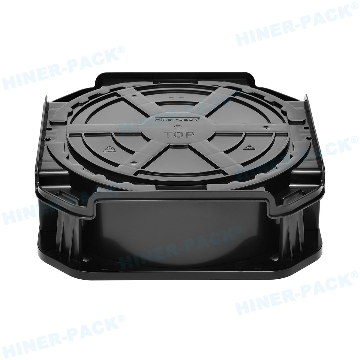
The "Waffle Pack" Tray Design
For diced dies, the waffle pack is the standard. These trays look like a grid of tiny pockets. Each pocket holds one die. The dimensions of the pocket are critical.
If the pocket is too large, the die will rotate or flip during transport. This is known as "die migration." If the die flips upside down, the pick-and-place machine at the assembly plant will fail to pick it up, stopping the line.
If the pocket is too small, the die might get stuck. The ejector pin used to push the die out might crack the silicon if it has to force the part free.
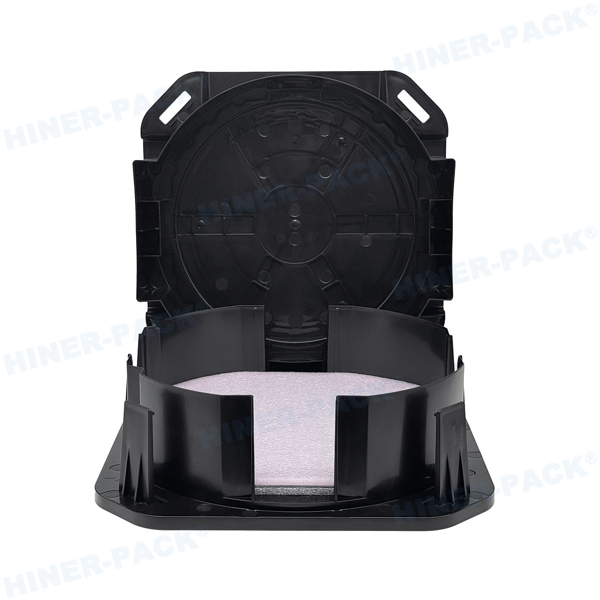
Gel and Vacuum Release Trays
Some wafer carrier trays do not use pockets. instead, they use a sticky gel membrane. These are known as Gel or VR (Vacuum Release) trays.
The wafer or dies sit on a proprietary gel material. The surface tension holds them in place. This is excellent for extremely fragile or oddly shaped components that don't fit into square pockets.
To release the parts, the machine applies a vacuum to the underside of the tray. The mesh below the gel pulls down, reducing the surface area of contact. The die pops loose and can be lifted. This technology is vital for photonics and ultra-thin MEMS devices.
Thermal Stability and Bakeable Trays
Moisture is an enemy of plastic packaging. Trays absorb water from the air. When these trays are placed in a high-temperature environment (like a reflow oven or a curing chamber), that water turns to steam and can warp the tray or damage the chips.
"Bakeable" trays are made from high-temperature plastics like MPPO (Modified Polyphenylene Oxide) or PEEK. These can withstand temperatures up to 150°C or more.
Fab managers use these trays to "bake out" moisture from the dies before sealing them in dry packs. If your process involves heat, ensuring your carrier vendor supplies JEDEC-standard bakeable trays is mandatory.
Dimensional Stability and Automation
Modern assembly lines are fully automated. A human hand rarely touches the tray. Machines use vision systems to locate the pocket and the die.
This means the tolerances on wafer carrier trays must be microscopic. The "pitch" (distance between pocket centers) cannot vary. If a tray is molded poorly, the pitch might drift by a fraction of a millimeter across the length of the tray.
By the time the machine reaches the last pocket in the row, that drift accumulates. The nozzle misses the die and crashes into the plastic rib. This damages the nozzle and destroys the tray. Consistent molding pressure and high-quality tooling are required to prevent this.
Cleanliness and Particulates
A tray acts as a source of contamination if not manufactured correctly. Lower-quality trays can have "flash" (excess plastic) or loose burrs from the molding process.
During vibration in a truck or plane, these burrs break off. They become dust inside the sealed bag. When the customer opens the pack, the dust settles on the bond pads of the chip. This prevents wire bonding and leads to device failure.
Top-tier suppliers wash and inspect their trays in cleanroom environments. It is worth asking your supplier about their washing protocols.
The Role of Hiner-pack in the Supply Chain
Sourcing these components can be difficult during market peaks. When semiconductor demand surges, plastic resin shortages often follow.
Working with established brands like Hiner-pack helps mitigate this risk. They typically maintain inventory buffers and have diverse raw material sourcing. Furthermore, their focus on consistent mold maintenance ensures that the trays bought in December fit the same machine settings as the ones bought in January. Consistency is the primary metric for long-term vendor relationships.
Horizontal Wafer Shippers (Coin Stack)
For whole wafers that have not been diced, "coin stack" shippers are a common variation of the carrier tray.
In this system, a bottom tray and a top cover sandwich a stack of wafers. Between each wafer, a separator tray or sheet is inserted.
These separators are crucial. They must be soft enough not to scratch the wafer surface but rigid enough to prevent the wafers from touching each other. Tyvek discs or ESD foam are often used in conjunction with plastic spacer rings.
Tape and Reel vs. Trays
Why use trays instead of Tape and Reel? Tape is faster for very small components (passives like resistors). However, for larger, high-value ICs (CPUs, GPUs, Sensors), wafer carrier trays offer better protection.
Trays are rigid. They protect the pins and corners of a BGA or QFP package. Tape is flexible and can bend, potentially stressing a large silicon die. Trays are also easier to reuse and recycle compared to the complex mix of plastics in a carrier tape reel.
Shipping Configurations
You don't just put a tray in a box and mail it. The standard shipping configuration involves a stack of trays.
A "cover tray" is placed on top. This is a flat lid that snaps onto the top carrier. The stack is then strapped together.
This unit is placed inside a Moisture Barrier Bag (MBB). A Desiccant pouch (to absorb moisture) and a Humidity Indicator Card (HIC) are added. The air is vacuumed out, and the bag is heat-sealed. This ensures the trays arrive at the destination in the exact same condition they left the cleanroom.
Recycling and Sustainability
The semiconductor industry generates a lot of plastic waste. Single-use packaging is becoming a regulatory target.
Many wafer carrier trays are designed for a closed-loop system. The customer receives the parts, empties the trays, and ships the empty trays back to the supplier or the fab for cleaning and reuse.
Materials like Carbon-loaded ABS are recyclable. However, regrinding the plastic can degrade its ESD properties. Manufacturers have to carefully blend recycled material with virgin resin to maintain the required electrical specifications.
Cost Considerations
There is always a temptation to buy the cheapest plastic tray available. This is often a false economy.
Cheap trays often use inconsistent recycled fillers. This leads to "hot spots" where the tray is not conductive, or areas where the carbon sloughs off as black dust.
The cost of cleaning a contaminated line or scrapping a batch of wafers far exceeds the savings on the packaging. Procurement teams should evaluate the "Total Cost of Ownership," which includes yield loss risk, rather than just the price per unit.
Customization Needs
Standard JEDEC trays fit most packages. But what if you have a custom sensor or a lens?
Custom wafer carrier trays require new tooling. The mold cost can be significant. However, a custom pocket ensures the part is supported exactly where it needs to be. For MEMS devices with suspended structures, custom trays are often the only way to ship without breakage.
Suppliers who offer rapid prototyping services for custom pockets are valuable partners during the NPI (New Product Introduction) phase.
Visual Inspection
Clear anti-static trays allow for visual inspection without opening the package. This is a significant advantage for quality control. Operators can check the part number and orientation through the plastic.
However, clear plastics that are also permanently anti-static are more expensive than black carbon-loaded plastics. This trade-off between visibility and cost is a common decision point for packaging engineers.
Final Thoughts on Selection
Selecting the right packaging is an engineering decision, not just a purchasing one. It requires understanding the mechanical sensitivity of the die, the electrical requirements of the circuit, and the capabilities of the pick-and-place machinery.
Whether you need a high-temp bakeable solution or a low-cost shipping tray, the market offers options. Companies like Hiner-pack continue to refine these designs, offering robust solutions that protect the industry's most valuable assets. By prioritizing material quality and dimensional precision, manufacturers can ensure their silicon survives the journey from the fab to the final device.
Common Questions (FAQ)
Q1: What is the difference between a JEDEC tray and a waffle pack?
A1: The terms are often used interchangeably, but "JEDEC tray" refers to a specific standardized footprint (approx 315mm x 136mm) defined by the JEDEC organization. This standard size fits almost all automated pick-and-place machines. A "waffle pack" is a generic term for any tray with a grid of pockets, but usually refers to the smaller 2-inch or 4-inch square trays used for bare die storage.
Q2: Can I re-use wafer carrier trays?
A2: Yes, trays can often be reused, but they must be cleaned and inspected first. You must check for physical damage (cracks, bent edges) and verify that the ESD coating has not worn off. Some high-precision trays are treated as single-use to avoid any risk of cross-contamination between batches.
Q3: Why are most chip trays black?
A3: Most wafer carrier trays are black because they are made with carbon additives (carbon powder or fiber). The carbon makes the plastic electrically conductive or dissipative, which prevents the buildup of static electricity that could destroy the sensitive chips inside.
Q4: What temperature can a standard tray withstand?
A4: Standard ABS or Polystyrene trays are rated for roughly 50°C to 60°C. They cannot be placed in an oven. If you need to bake the moisture out of your components while they are in the tray, you must buy "high-temp" or "bakeable" trays, usually made of MPPO or PSU, which can withstand 125°C to 150°C.
Q5: How do I know which pocket size to choose for my die?
A5: The pocket size should be slightly larger than the die to allow for easy insertion, but tight enough to prevent rotation. A common rule of thumb is to have a clearance of roughly 0.05mm to 0.1mm on the sides. The depth is also important; the die should sit below the top surface of the tray so the lid doesn't crush it. Suppliers usually provide a catalog of standard pocket dimensions to match your die size.


