
Within the intricate ecosystem of semiconductor manufacturing, every component that contacts a silicon wafer carries significant responsibility. While front-opening unified pods (FOUPs) dominate 300mm automated transport, semiconductor wafer trays remain indispensable workhorses. They are used for smaller diameter wafers, during specific process steps, in metrology, for transportation between facilities, and in R&D or back-end operations. More than simple carriers, these trays are precision-engineered tools. Their primary job is to ensure wafers remain secure, contamination-free, and undamaged during manual or automated handling, storage, and transport. Selecting the right tray is a critical decision that impacts yield and operational efficiency. Manufacturers like Hiner-pack specialize in producing these vital components, understanding that their design and material directly influence production outcomes.
The Critical Role of Wafer Trays in Fabrication
Why is so much attention paid to what seems like a simple holder? The answer lies in the extreme value and fragility of the wafers themselves. A semiconductor wafer tray provides the first line of physical defense.
Its functions are multifaceted:
- Physical Support: It cradles the wafer, preventing flexing, chipping, or cracking at the edge, which is particularly vulnerable.
- Contamination Control: The tray material must not generate particles or outgas chemicals that could settle on the wafer surface.
- Process Compatibility: Trays must withstand various fab environments, including exposure to chemicals, high temperatures in furnaces, or UV light.
- Handling Efficiency: They enable safe, batch handling of multiple wafers, speeding up logistics and reducing individual touchpoints.
A poorly designed tray can introduce defects, leading to costly scrap. Therefore, engineers treat tray selection as a key part of process design.
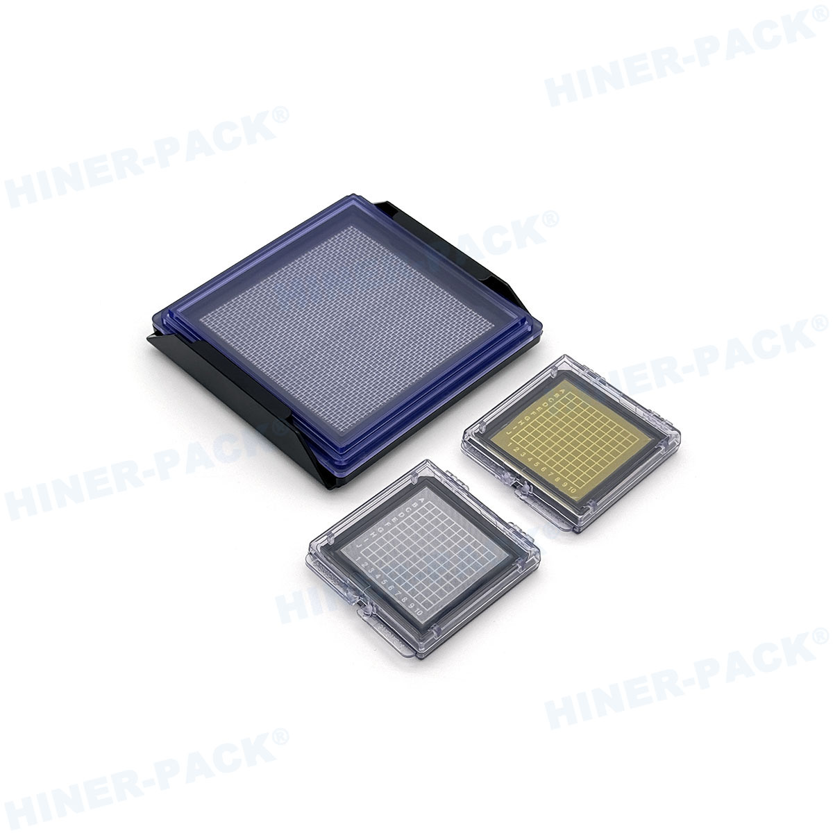
Common Types of Semiconductor Wafer Trays
Not all wafer trays serve the same purpose. The design varies significantly based on the wafer size, process step, and handling method.
Cassettes and Boats
These are the most recognizable types, often used in vertical furnaces or wet benches.
- Quarter-Moon or Boat Trays: Designed for high-temperature processes like diffusion or oxidation. They hold wafers in a vertical, slightly angled position and are typically made from pure quartz or silicon carbide to withstand extreme heat.
- Cassettes: Used for horizontal batch processing in cleaning or etching baths. They are usually open-structured to allow chemicals and rinsing water to flow freely over the wafers. Materials include PTFE (Teflon) or PFA for excellent chemical resistance.
Front-Opening Shipping Boxes (FOSB) & Transport Trays
For safely moving wafers between fabs or across long distances, sturdier containers are needed.
- FOSBs: These are sealed, rigid boxes for 300mm wafers, providing mechanical and environmental protection during air or road freight. They often include cushioning and environmental monitors.
- Small-Diameter Transport Trays: For 150mm or 200mm wafers, these are robust, latchable plastic trays with precise wafer slots and sometimes foam liners. They are crucial for the supply chain of epitaxial wafers or finished wafers sent to assembly and test facilities.
Specialty and Measurement Trays
Some trays are built for very specific tasks.
- Vacuum Chuck Trays: Used in metrology tools, these trays hold wafers flat on a vacuum chuck during measurement, ensuring no back-side contamination.
- JEDEC Trays: Standardized trays used in the back-end for handling diced wafers or chips, compatible with pick-and-place equipment.
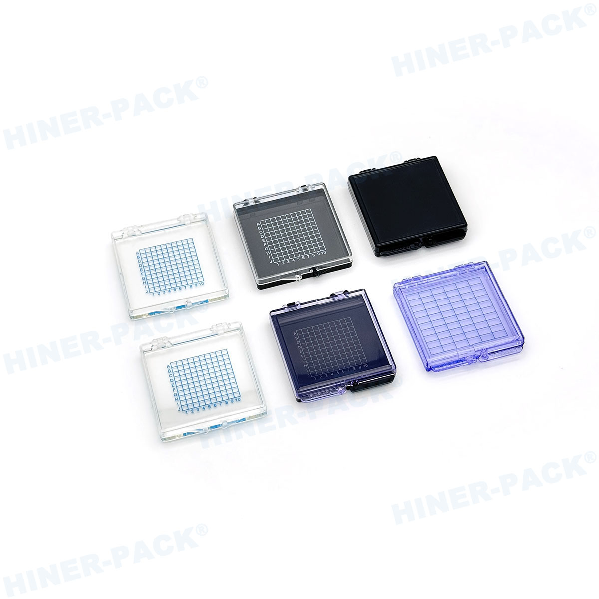
Material Considerations: Balancing Performance
The choice of material for a semiconductor wafer tray is a careful balance of purity, durability, and cost. Each material brings distinct advantages.
- Polypropylene (PP) and Polycarbonate (PC):PP: Cost-effective, good chemical resistance, and low particulate generation. Common for general-purpose handling and storage of less sensitive wafers.PC: Offers higher clarity and better rigidity than PP. Often used where visual inspection of wafers in the tray is necessary.
- PFA, PTFE, and other Fluoropolymers:These are the gold standard for harsh chemical environments. They exhibit exceptional purity, minimal outgassing, and resistance to nearly all process chemicals. They are preferred for critical cleaning and etching steps, though they come at a higher cost.
- Quartz and Silicon Carbide:Essential for high-temperature processes exceeding 1000°C. These ceramic materials do not warp or contaminate wafers at extreme heat. Quartz boats are transparent, while silicon carbide offers greater durability.
- PEEK (Polyether Ether Ketone):A high-performance engineering plastic. PEEK offers an excellent balance of thermal stability (up to 250°C continuously), mechanical strength, and chemical resistance. It is a premium choice for demanding applications where fluoropolymers might be too soft or standard plastics cannot withstand the heat.
Suppliers like Hiner-pack work with a range of these materials, often offering options like static-dissipative compounds to prevent electrostatic discharge (ESD) risks, which is a critical feature for modern devices.
How to Select the Right Wafer Tray for Your Process
Choosing a tray is not a one-size-fits-all decision. It requires a methodical assessment of your specific needs.
Ask these key questions:
- Wafer Size and Thickness? The tray must have precise slot dimensions to prevent movement or stress.
- Process Environment? Will the tray see acids, solvents, DI water, high heat, or UV light? The material must be compatible.
- Automation Compatibility? Does the tray need to interface with a robotic arm or conveyor system? Specific notches and dimensions may be required.
- Cleanroom Class? For ISO Class 3 and better, only the highest-purity, low-outgassing materials like PFA or premium PEEK are suitable.
- Static Sensitivity? For advanced nodes, ESD-protective materials are mandatory to prevent latent damage.
Always consult with your equipment manuals and consider running qualification tests with sample trays from your supplier. The upfront time investment prevents downstream yield issues.
Maintenance and Cleaning Protocols
Even the best tray will become a contamination source if not properly maintained. A clear cleaning and inspection regimen is essential.
- Establish a Cleaning Schedule: Frequency depends on use. Trays in wet benches may need cleaning after each run, while storage trays might be cleaned weekly.
- Use Approved Cleanroom Methods: This typically involves ultrasonic baths with specialized semiconductor-grade solvents (like DI water with specific chemistry), followed by thorough rinsing and drying in a particle-free environment.
- Implement Regular Inspection: Check trays for visible particles, chemical residue, cracks, or warping. Worn or damaged trays must be taken out of service immediately.
- Proper Storage: Clean trays should be stored in sealed, clean containers or bags when not in use to prevent recontamination.
In the meticulous world of chip making, success is built on a foundation of reliable, precision components. Semiconductor wafer trays are a perfect example of an unsung hero. Their quiet role in supporting, protecting, and transporting valuable wafers is fundamental to maintaining high yields and smooth fab operations. From the chemical resistance of a PFA cassette to the thermal stability of a quartz boat, each tray is engineered to solve a specific set of challenges. By carefully selecting the correct type and material for your application—and partnering with experienced manufacturers who understand these nuances—you invest directly in process stability and product quality. As a trusted provider in this space, Hiner-pack offers the material expertise and manufacturing precision necessary for these critical containment solutions.
Frequently Asked Questions (FAQs)
Q1: What is the main difference between a wafer cassette and a wafer boat?
A1: The primary difference lies in their typical use. A wafer boat (or quarter-moon boat) is designed for high-temperature vertical furnace processes. It's usually made of quartz or silicon carbide. A cassette is typically used for horizontal processing in wet stations (cleaning, etching) and is often made from chemically resistant plastics like PTFE or PFA. The cassette's open structure allows for fluid flow.
Q2: How often should I clean my polypropylene or PFA wafer trays?
A2: There is no universal rule; it depends on your process contamination data. A common practice is to clean trays after each process run for critical steps, or whenever visual inspection or particle count monitors indicate a buildup. Establish a baseline schedule (e.g., every 5 or 10 uses) and adjust based on your facility's quality control metrics.
Q3: Can wafer trays be used in automated material handling systems (AMHS)?
A3: Yes, but they require specific design features. Trays meant for automation will have precise external dimensions, alignment notches, and sometimes machine-readable barcodes. Standard manual-handling trays may not fit or interface correctly with robotic systems. Always verify compatibility with your AMHS specifications.
Q4: Are there industry standards for wafer tray dimensions?
A4: Yes, for certain applications. SEMI (Semiconductor Equipment and Materials International) publishes standards for various wafer packaging and carrier dimensions. For example, SEMI Standard E1.2 outlines specifications for 150mm plastic shipping boxes. Using trays that comply with relevant SEMI standards ensures interoperability between equipment from different vendors.
Q5: Why is static dissipation important in a wafer tray?
A5: Electrostatic discharge (ESD) or charge buildup can attract airborne particles to the wafer surface, causing defects. More severely, it can directly damage or degrade sensitive microcircuits, a failure that might not be detected until final testing. Static-dissipative trays safely bleed away any accumulated charge, protecting the wafer throughout handling and storage.


