
In the fast-paced world of semiconductor manufacturing, every component plays a critical role in ensuring the integrity and yield of delicate silicon wafers. Among these, the silicon wafer box stands out as a fundamental element in safeguarding wafers during storage, transport, and processing. This article delves into the importance of silicon wafer boxes, explores various silicon wafer packaging solutions, highlights the benefits of custom silicon wafer box options, discusses the necessity of FOUP cleaning service, and provides insights into selecting a reliable silicon wafer box manufacturer. By understanding these aspects, industry professionals can optimize their operations, reduce contamination risks, and improve overall productivity. As semiconductor technology advances, the demand for robust and tailored packaging solutions continues to grow, making it essential to stay informed about the latest innovations and best practices. Whether you're involved in fabrication, assembly, or testing, this overview will equip you with valuable knowledge to make informed decisions.
The Role of Silicon Wafer Box in Modern Semiconductor Industry
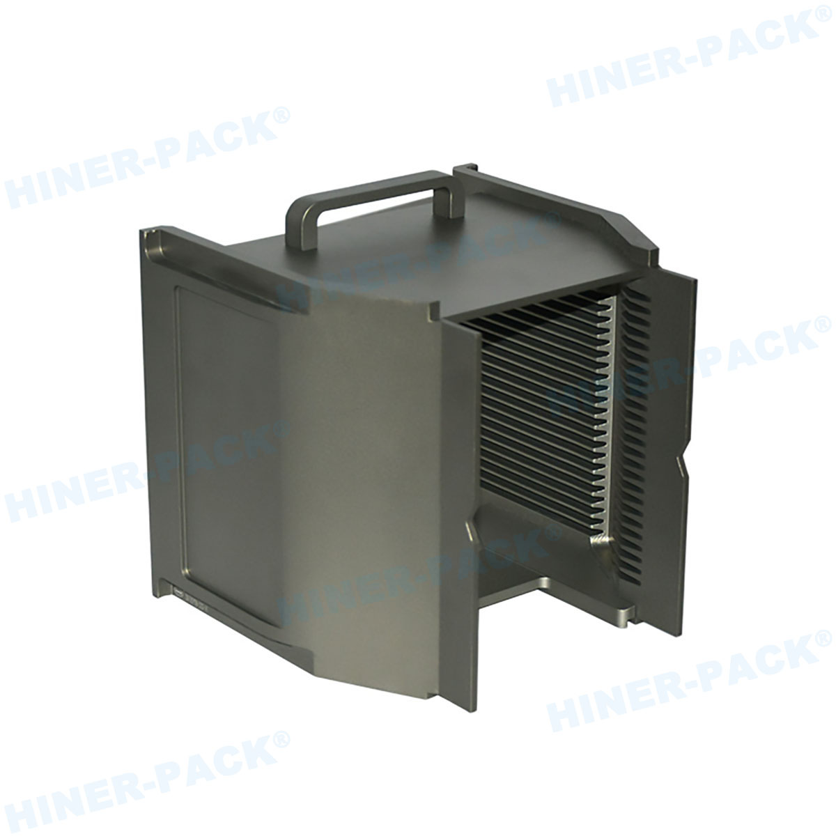
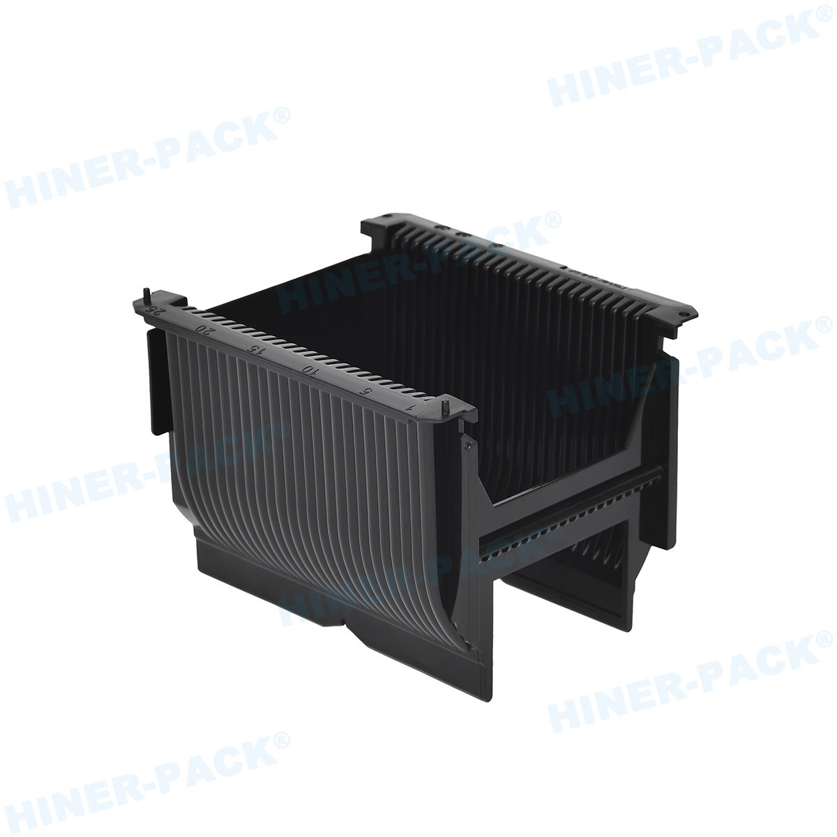
A silicon wafer box, often referred to as a FOUP (Front Opening Unified Pod) or cassette, is a specialized container designed to hold and protect silicon wafers from environmental contaminants, physical damage, and electrostatic discharge. These boxes are crucial in cleanroom environments where even microscopic particles can compromise wafer quality and lead to significant financial losses. Typically made from high-purity materials like polycarbonate or PEEK, a silicon wafer box ensures that wafers remain in a controlled atmosphere, maintaining their electrical properties and surface integrity throughout the manufacturing process. The design of a silicon wafer box includes features such as secure locking mechanisms, RFID tags for tracking, and ergonomic handles for easy handling. In today's competitive landscape, the efficiency of a silicon wafer box directly impacts production timelines and yield rates, making it a vital component in semiconductor facilities worldwide. By integrating advanced silicon wafer packaging solutions, companies can achieve higher throughput and better compliance with industry standards like SEMI.
Exploring Silicon Wafer Packaging Solutions for Optimal Performance
Silicon wafer packaging solutions encompass a range of products and strategies aimed at protecting wafers from fabrication to end-use. These solutions include not only standard silicon wafer boxes but also specialized containers, trays, and shipping materials that cater to different wafer sizes, such as 200mm, 300mm, or emerging 450mm formats. Key aspects of effective silicon wafer packaging solutions involve contamination control, mechanical stability, and compatibility with automated handling systems. For instance, anti-static properties and low outgassing materials are essential to prevent wafer damage during transit. Additionally, modular designs allow for customization based on specific process requirements, such as high-temperature resistance or UV protection. By adopting comprehensive silicon wafer packaging solutions, manufacturers can minimize defects, reduce downtime, and enhance scalability. This approach often involves collaboration with experts in silicon wafer box manufacturer fields to ensure that solutions align with evolving technological demands, such as those in IoT, AI, and 5G applications.
Benefits of Investing in a Custom Silicon Wafer Box
A custom silicon wafer box offers tailored advantages that standard options cannot match, addressing unique operational challenges in semiconductor production. By working with a skilled silicon wafer box manufacturer, companies can design boxes with specific dimensions, materials, and features to suit their exact needs. For example, a custom silicon wafer box might include integrated sensors for real-time monitoring of temperature and humidity, or specialized compartments for handling fragile wafers with minimal contact. This level of customization not only improves protection but also boosts efficiency by streamlining workflows and reducing manual interventions. In high-volume facilities, a custom silicon wafer box can lead to significant cost savings by lowering breakage rates and extending the lifespan of wafers. Moreover, it supports compliance with stringent regulatory requirements, such as those in the medical or aerospace sectors. When considering a custom silicon wafer box, it's important to evaluate factors like lead times, scalability, and testing protocols to ensure optimal performance. Ultimately, investing in a custom solution can be a game-changer for businesses aiming to stay ahead in the competitive semiconductor market.
The Importance of FOUP Cleaning Service in Maintaining Wafer Integrity
FOUP cleaning service is an essential maintenance practice that ensures silicon wafer boxes remain free from contaminants that could otherwise transfer to wafers. Over time, residues from processing chemicals, particles, and biological matter can accumulate inside a silicon wafer box, posing a risk to wafer purity. Regular FOUP cleaning service involves using advanced techniques like ultrasonic cleaning, chemical baths, and dry methods to remove these impurities without damaging the box's structure. This process is critical in preventing cross-contamination between batches and maintaining the high standards required in cleanroom environments. Many silicon wafer box manufacturer companies offer integrated FOUP cleaning service as part of their product support, providing scheduled maintenance and emergency cleaning to minimize downtime. By incorporating a reliable FOUP cleaning service into their routines, semiconductor facilities can extend the life of their silicon wafer boxes, reduce replacement costs, and uphold consistent yield rates. It's recommended to follow industry guidelines, such as those from SEMI, for cleaning frequencies and methods to achieve the best results.
How to Choose a Reliable Silicon Wafer Box Manufacturer
Selecting the right silicon wafer box manufacturer is a critical decision that impacts the quality, reliability, and cost-effectiveness of your semiconductor operations. A reputable silicon wafer box manufacturer should have a proven track record in producing high-quality boxes that meet international standards, such as ISO 14644 for cleanroom compatibility. Key factors to consider include the manufacturer's expertise in materials science, their ability to provide custom silicon wafer box options, and their support services like FOUP cleaning service. It's also important to assess their production capabilities, such as whether they use injection molding or additive manufacturing, and their quality control processes, including testing for durability and contamination resistance. Additionally, look for manufacturers who offer comprehensive customer support, including technical assistance and after-sales service. By partnering with a trusted silicon wafer box manufacturer, you can ensure a steady supply of reliable packaging solutions that align with your production goals. Don't hesitate to request samples or visit facilities to verify their claims, as this can help avoid potential issues down the line.
Integrating Silicon Wafer Packaging Solutions into Your Workflow
To maximize the benefits of silicon wafer packaging solutions, it's crucial to integrate them seamlessly into your existing workflows. This involves training staff on proper handling procedures, implementing inventory management systems for tracking silicon wafer boxes, and regularly auditing processes for contamination control. For instance, using a combination of standard and custom silicon wafer box designs can optimize space utilization in storage areas and transport vehicles. Collaboration with a silicon wafer box manufacturer can provide insights into best practices for integration, such as automating box retrieval systems or incorporating IoT devices for real-time monitoring. Moreover, aligning these solutions with FOUP cleaning service schedules ensures that boxes are always ready for use without interrupting production. By taking a holistic approach, companies can achieve a more efficient and resilient supply chain, reducing risks associated with wafer damage and delays. This integration not only supports operational excellence but also fosters innovation by allowing teams to focus on core development activities rather than logistical challenges.
Future Trends in Silicon Wafer Box Technology
The evolution of silicon wafer box technology is driven by the increasing demands for smaller, more powerful semiconductors. Future trends may include the adoption of smart silicon wafer boxes embedded with AI and IoT sensors to provide predictive analytics on wafer health and environmental conditions. These advancements will likely be supported by innovations in materials, such as graphene-based composites, which offer superior strength and contamination resistance. Additionally, as sustainability gains importance, we may see a shift toward eco-friendly silicon wafer packaging solutions that use recyclable materials and energy-efficient production methods. A forward-thinking silicon wafer box manufacturer will be at the forefront of these developments, offering products that not only meet current needs but also anticipate future challenges. By staying updated on these trends, semiconductor companies can proactively adapt their strategies, ensuring long-term competitiveness and compliance with global standards.
In conclusion, the silicon wafer box is more than just a container; it is a pivotal component in the semiconductor ecosystem that directly influences yield, efficiency, and innovation. From exploring diverse silicon wafer packaging solutions to leveraging custom silicon wafer box designs and maintaining hygiene through FOUP cleaning service, every aspect contributes to operational success. Partnering with a reliable silicon wafer box manufacturer ensures access to high-quality products and support services that keep pace with industry evolution. As technology continues to advance, embracing these elements will be key to thriving in the competitive semiconductor landscape. By prioritizing the protection and management of silicon wafers, businesses can unlock new levels of performance and reliability.
Frequently Asked Questions (FAQ)
Q1: What is the primary purpose of a silicon wafer box?
A1: The primary purpose of a silicon wafer box is to protect silicon wafers from contamination, physical damage, and electrostatic discharge during storage, transport, and processing in semiconductor manufacturing. It helps maintain wafer integrity by providing a controlled environment, which is essential for high yield and quality in production.
Q2: How does a custom silicon wafer box differ from standard options?
A2: A custom silicon wafer box is tailored to specific operational needs, such as unique dimensions, materials, or integrated features like sensors for monitoring conditions. In contrast, standard boxes are mass-produced with general specifications. Custom options offer enhanced protection, efficiency, and compatibility with specialized processes, often resulting in cost savings and improved performance.
Q3: Why is FOUP cleaning service important for semiconductor facilities?
A3: FOUP cleaning service is important because it removes contaminants that accumulate in silicon wafer boxes over time, preventing cross-contamination and ensuring wafer purity. Regular cleaning extends the box's lifespan, reduces the risk of defects, and supports consistent production yields, making it a critical maintenance practice in cleanroom environments.
Q4: What should I look for when selecting a silicon wafer box manufacturer?
A4: When selecting a silicon wafer box manufacturer, consider factors such as their experience, compliance with industry standards (e.g., SEMI or ISO), ability to provide custom solutions, quality control processes, and additional services like FOUP cleaning service. It's also beneficial to review their customer support, production capabilities, and track record for reliability.
Q5: How often should silicon wafer boxes be cleaned or replaced?
A5: The frequency of cleaning or replacing silicon wafer boxes depends on usage intensity and contamination levels, but generally, FOUP cleaning service should be performed regularly—often after each use or according to a scheduled maintenance plan—based on industry guidelines. Replacement may be needed when boxes show signs of wear, such as cracks or reduced performance, typically after several years of use, but this can vary with handling and environmental conditions.


