
In the highly precise world of semiconductor fabrication, the 200mm wafer carrier plays an indispensable role in ensuring the safe transport and storage of silicon wafers. As the industry continues to rely on 200mm wafers for various applications, from power devices to sensors, understanding the components surrounding these carriers—including 200mm FOUP manufacturers, cleaning equipment, and maintenance protocols—is vital for maintaining yield and minimizing contamination. This article delves into the essentials of 200mm wafer carriers, covering key aspects like manufacturers, cleaning equipment, and best practices for upkeep. By exploring these areas, professionals can enhance their operational efficiency and prolong the lifespan of their equipment.
What is a 200mm Wafer Carrier?
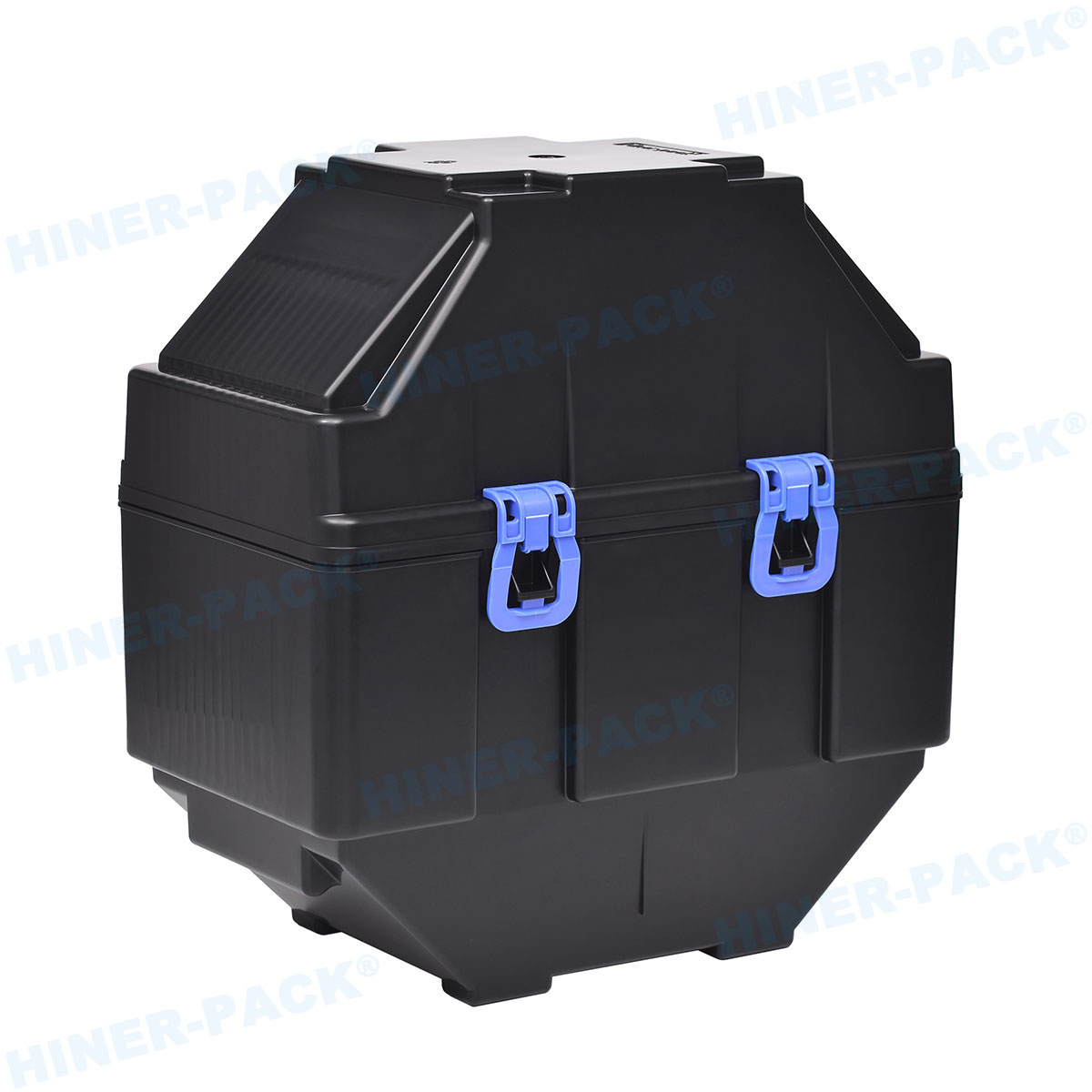
A 200mm wafer carrier, often referred to as a Front Opening Unified Pod (FOUP) in advanced contexts, is a specialized container designed to hold and protect 200mm silicon wafers during processing, transportation, and storage in semiconductor facilities. These carriers are critical for preventing contamination, physical damage, and electrostatic discharge, which could compromise the integrity of the wafers. Typically made from materials like polycarbonate or other high-purity plastics, 200mm wafer carriers are engineered to meet strict industry standards for cleanliness and durability. They feature precise docking mechanisms and are compatible with automated handling systems, ensuring seamless integration into fabrication lines. The evolution of the 200mm wafer carrier has been driven by the need for higher throughput and reduced particle counts, making it a cornerstone in fabs that still utilize 200mm technology for cost-effective production.
Key 200mm FOUP Manufacturers in the Industry
When it comes to sourcing reliable 200mm wafer carriers, the role of 200mm FOUP manufacturers cannot be overstated. These companies specialize in designing and producing carriers that meet the rigorous demands of semiconductor environments. Leading 200mm FOUP manufacturers include global players like Entegris, Inc., which offers a range of carriers with advanced materials to minimize contamination and maximize durability. Another prominent name is Shin-Etsu Polymer, known for their innovative FOUP designs that enhance wafer protection and handling efficiency. Additionally, companies such as Miraial and Gudeng Precision provide customized solutions tailored to specific fab requirements, including anti-static properties and improved sealing mechanisms. The competition among 200mm FOUP manufacturers has led to advancements in carrier technology, such as reduced weight for easier automation and enhanced thermal stability for high-temperature processes. By partnering with reputable 200mm FOUP manufacturers, fabs can ensure consistent performance and reduce downtime due to carrier-related issues. It's essential for buyers to evaluate factors like material purity, certification standards, and after-sales support when selecting a supplier, as these elements directly impact the overall efficiency and cost-effectiveness of semiconductor operations.
Overview of 200mm FOUP Cleaning Equipment
Maintaining the cleanliness of 200mm wafer carriers is paramount, and this is where specialized 200mm FOUP cleaning equipment comes into play. This equipment is designed to remove contaminants such as particles, residues, and molecular films that accumulate during wafer processing. Common types of 200mm FOUP cleaning equipment include automated wet benches, dry cleaning systems, and ultrasonic cleaners, each tailored to address specific contamination challenges. For instance, wet cleaning systems often use deionized water and high-purity chemicals to dissolve organic and inorganic residues, while dry methods like plasma cleaning can effectively remove thin films and volatile compounds without introducing moisture. Advanced 200mm FOUP cleaning equipment may incorporate features like robotic arms for handling, real-time monitoring sensors, and HEPA-filtered environments to prevent recontamination. Brands like Screen Holdings and Lam Research offer state-of-the-art solutions that integrate with fab automation, ensuring consistent cleaning cycles and minimal human intervention. The adoption of reliable 200mm FOUP cleaning equipment is crucial for meeting industry standards like SEMI guidelines, which dictate maximum allowable particle counts. By investing in high-quality 200mm FOUP cleaning equipment, fabs can extend the life of their carriers, reduce defect rates, and maintain high yields in 200mm wafer production lines.
How to Clean a 200mm Wafer Carrier: A Step-by-Step Process
Knowing how to clean 200mm wafer carrier units effectively is essential for any semiconductor facility aiming to uphold strict cleanliness protocols. The process typically involves several meticulous steps to ensure all contaminants are eradicated without damaging the carrier. Here's a comprehensive guide on how to clean 200mm wafer carrier:
Pre-Cleaning Inspection: Begin by visually inspecting the 200mm wafer carrier for any visible debris, scratches, or damage. Use a laminar flow bench to avoid introducing new particles during handling.
Disassembly (if applicable): If the carrier design allows, disassemble removable parts like doors and liners to access hard-to-reach areas. This step is critical for thorough cleaning, especially in carriers used in high-contamination processes.
Initial Rinsing: Rinse the carrier with deionized water to remove loose particles and soluble residues. This pre-rinse helps reduce the load on subsequent cleaning stages and minimizes chemical usage.
Chemical Cleaning: Apply a specialized cleaning solution, such as isopropyl alcohol or a neutral detergent, using automated spray systems or immersion baths. Agitate the solution to enhance contact with surfaces, and ensure the chemicals are compatible with the carrier material to prevent degradation.
Ultrasonic or Megasonic Cleaning: For stubborn contaminants, use ultrasonic or megasonic cleaners that generate high-frequency sound waves to dislodge particles from microscopic pores. This step is particularly effective for 200mm wafer carrier cleaning in applications involving photoresist or etch residues.
Final Rinsing and Drying: Rinse thoroughly with deionized water to remove any chemical traces, followed by a drying phase using nitrogen gas or heated air in a controlled environment. Ensure the carrier is completely dry to prevent moisture-related issues like corrosion or bacterial growth.
Reassembly and Verification: Reassemble the carrier if disassembled, and conduct a final inspection using particle counters or surface analysis tools. Document the cleaning process for quality assurance and traceability.
By following these steps on how to clean 200mm wafer carrier, technicians can maintain carrier integrity and support continuous production without interruptions. Regular training and adherence to standardized procedures are key to mastering this process.
Best Practices for 200mm Wafer Carrier Cleaning
Implementing best practices for 200mm wafer carrier cleaning is crucial for achieving optimal results and minimizing operational costs. First, establish a routine cleaning schedule based on usage patterns and contamination levels—for example, carriers exposed to high-particle processes may require daily cleaning, while others might be serviced weekly. Use validated 200mm FOUP cleaning equipment that aligns with SEMI standards to ensure consistency and reproducibility. It's also important to monitor cleaning agents for purity and replace them regularly to avoid cross-contamination. Additionally, incorporate preventive measures such as storing carriers in clean environments and using dedicated tools for handling to reduce pre-cleaning contamination. Another key aspect of 200mm wafer carrier cleaning is personnel training; ensure that staff are well-versed in proper techniques and safety protocols to handle chemicals and equipment safely. Data logging and analysis can further enhance 200mm wafer carrier cleaning efforts by identifying trends in contamination and optimizing cleaning parameters. By adopting these best practices, fabs can not only improve carrier performance but also contribute to overall fab hygiene and product yield.
Common Challenges and Solutions in 200mm Wafer Carrier Maintenance
Despite advances in technology, maintaining 200mm wafer carriers presents several challenges. One common issue is the accumulation of hard-to-remove residues, such as polymers from plasma processes, which can require specialized 200mm FOUP cleaning equipment or alternative chemistries. Another challenge is the wear and tear on carrier components over time, leading to misalignment or seal failures that compromise containment. To address this, regular inspections and proactive replacement of worn parts are recommended. Contamination from human handling is also a concern, which can be mitigated through automation and the use of gloves and cleanroom apparel. Furthermore, variations in cleaning efficacy across different 200mm FOUP manufacturers' designs may necessitate customized cleaning protocols. By collaborating with 200mm FOUP manufacturers and leveraging data-driven maintenance strategies, fabs can overcome these hurdles and ensure their 200mm wafer carriers remain in peak condition.
The Future of 200mm Wafer Carrier Technology
As the semiconductor industry evolves, so does the technology surrounding 200mm wafer carriers. Innovations from 200mm FOUP manufacturers are focusing on smarter carriers embedded with sensors for real-time monitoring of contamination levels and environmental conditions. These "intelligent" carriers could revolutionize 200mm wafer carrier cleaning by providing data that triggers automated cleaning cycles, reducing manual intervention. Additionally, advancements in materials science may lead to carriers with self-cleaning surfaces or enhanced resistance to chemicals and heat. The integration of IoT and AI into 200mm FOUP cleaning equipment is also on the horizon, enabling predictive maintenance and optimized resource usage. Despite the shift toward larger wafer sizes, the demand for 200mm technology remains strong in niche markets, ensuring that 200mm wafer carriers will continue to be a vital component. By staying abreast of these trends, industry players can future-proof their operations and maintain competitiveness.
Frequently Asked Questions (FAQ)
Q1: What is the primary function of a 200mm wafer carrier?
A1: The primary function of a 200mm wafer carrier is to safely transport, store, and protect 200mm silicon wafers from contamination, physical damage, and electrostatic discharge during semiconductor manufacturing processes. It ensures wafers remain in a controlled environment, maintaining their integrity until they are used in fabrication steps.
Q2: How often should 200mm wafer carriers be cleaned?
A2: The frequency of cleaning 200mm wafer carriers depends on usage intensity and the specific processes they are exposed to. In high-contamination environments, cleaning may be required after every use or on a daily basis, while in less critical applications, a weekly or monthly schedule might suffice. Regular monitoring of particle counts can help determine the optimal cleaning interval.
Q3: What types of contaminants are commonly found in 200mm wafer carriers?
A3: Common contaminants include particulate matter (e.g., dust and debris), organic residues (such as oils and photoresist), inorganic films (like oxides and metals), and molecular contaminants from process gases. These can originate from handling, processing equipment, or environmental factors, and they must be removed through thorough 200mm wafer carrier cleaning to prevent wafer defects.
Q4: Can 200mm FOUP cleaning equipment be used for other wafer sizes?
A4: While some 200mm FOUP cleaning equipment may be adaptable, it is generally designed specifically for 200mm carriers due to size and compatibility requirements. Using it for other wafer sizes, such as 300mm, could lead to improper cleaning or damage. It's advisable to use equipment tailored to the specific carrier dimensions to ensure effectiveness and safety.
Q5: What are the key factors to consider when selecting a 200mm FOUP manufacturer?
A5: When selecting a 200mm FOUP manufacturer, consider factors such as the quality and purity of materials used, compliance with industry standards (e.g., SEMI), customization options, reliability and durability of the carriers, after-sales support, and cost-effectiveness. Evaluating the manufacturer's track record and customer reviews can also provide insights into their performance and product suitability for your fab needs.
In conclusion, the 200mm wafer carrier remains a foundational element in semiconductor manufacturing, with its effectiveness hinging on robust support from 200mm FOUP manufacturers, advanced 200mm FOUP cleaning equipment, and diligent cleaning practices. By understanding how to clean 200mm wafer carrier units and implementing best practices, fabs can achieve higher yields and reduce costs. As technology progresses, continuous improvement in these areas will be essential for sustaining the viability of 200mm wafer production in the global market.


