
In the high-stakes world of semiconductor manufacturing, where a single dust particle or electrostatic discharge (ESD) can render a multi-million-dollar wafer batch useless, protection is paramount. While much attention is given to lithography and etching tools, the humble wafer shipping box is a first-line defender against a silent, invisible threat: static electricity. This article delves into why anti static wafer boxes are not just containers, but sophisticated, essential components in the semiconductor supply chain.
Understanding the Invisible Enemy: Electrostatic Discharge (ESD)
Before appreciating the solution, one must understand the problem. Electrostatic discharge is the sudden flow of electricity between two electrically charged objects. In a fab or cleanroom environment, this can be caused by contact, separation, or even just proximity. The human body can easily generate static charges of several thousand volts, enough to damage or destroy sensitive microchips and integrated circuits (ICs) on a wafer.
The damage from ESD can be catastrophic and insidious. It can be:
Catastrophic Failure: An immediate and total failure of the circuit.
Latent Defect: A partial degradation that weakens the device, causing it to fail prematurely in the field, which is often more costly and damaging to brand reputation.
This is where robust ESD protection, starting with proper storage and transportation, becomes non-negotiable.
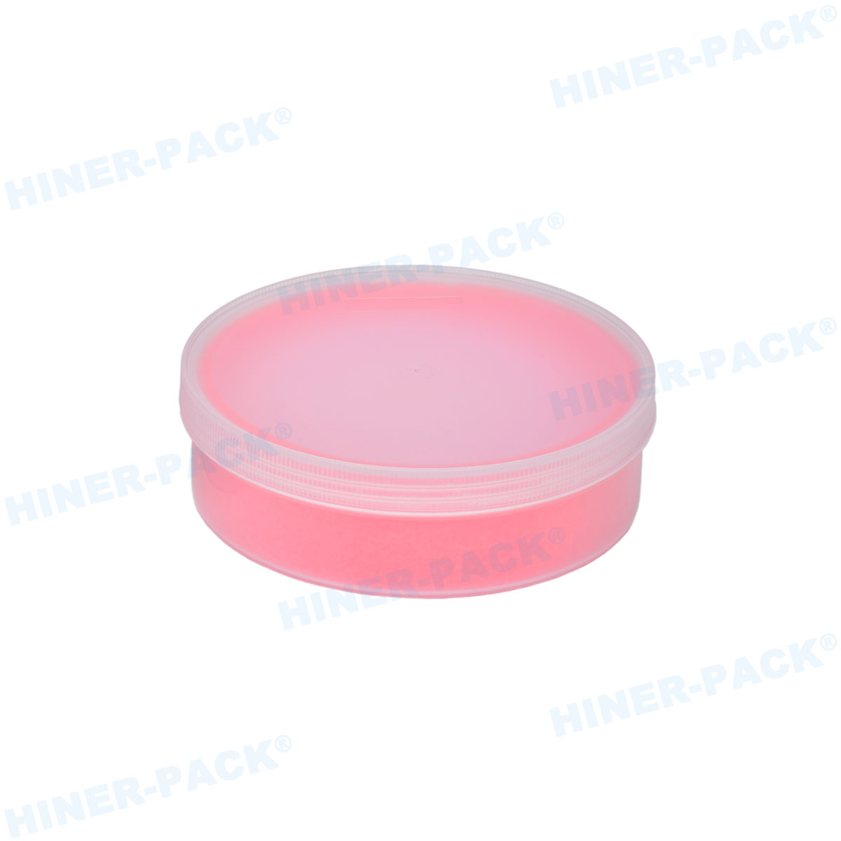
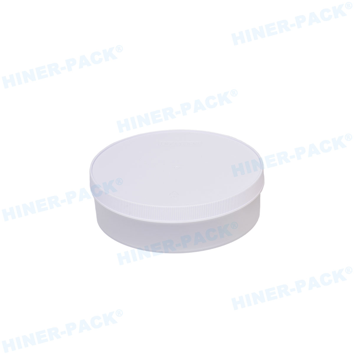
More Than Just a Box: The Materials and Design of Modern Wafer Carriers
A standard plastic container simply won't suffice. True anti static wafer boxes are engineered from specialized materials with specific properties. The primary goal is to either dissipate static charge safely to ground or to shield the wafers from external ESD events.
1. Material Science: Dissipative vs. Conductive
The most common materials used are:
Carbon-Loaded Polypropylene (PP): This creates a static dissipative material. It allows a controlled, slow bleed-off of static charge, preventing a rapid discharge that could damage wafers.
Polycarbonate (PC) and PEEK: These high-performance plastics are often used in combination with carbon or other additives to achieve the necessary ESD properties and physical robustness. PEEK, in particular, is valued for its high temperature resistance, crucial for post-process wafers.
Brands like Hiner-pack meticulously select and compound their raw materials to ensure consistent volume resistivity, typically in the range of 10^6 to 10^9 ohm-cm, which is the ideal anti static zone for safely dissipating charge without being overly conductive.
2. Shielding and Mechanical Protection
Beyond static dissipation, premium wafer shipping boxes provide electromagnetic interference (EMI) and radio frequency interference (RFI) shielding. This is achieved by incorporating a layer of conductive material, such as metal, into the box structure. Furthermore, the mechanical design is critical. Features include:
Precise Rib Supports: To cradle wafers without causing mechanical stress or particle generation.
Secure Latching Mechanisms: To prevent accidental opening during transit.
Stackability: Designed to be safely stacked without putting pressure on the contents of the box below.
Compliance and Standards: Ensuring Interoperability and Safety
The semiconductor industry is global and standardized. Any anti static wafer box must comply with key standards to ensure it functions correctly within the ecosystem. The most important governing body is SEMI.
SEMI Standards: SEMI defines everything from the physical dimensions of the boxes (e.g., for 200mm, 300mm, and now 450mm wafers) to the specific ESD performance requirements. Compliance with standards like SEMI E1.9 for 150mm carriers or the relevant standards for 200mm and 300mm boxes is a baseline requirement. Hiner-pack designs its products to meet or exceed these critical SEMI standards, ensuring seamless integration into automated material handling systems (AMHS) worldwide.
Applications Beyond Shipping: A Constant Guardian
While the name "wafer shipping box" implies a primary role in logistics, these containers are used throughout the wafer's life cycle.
Inter-Bay Transfer: Moving wafers between different process areas within a fab.
Temporary Storage: Holding wafers in queue before or after a specific process step.
Long-Term Archiving: For storing qualified wafers or device master wafers for extended periods.
In each scenario, the ESD safe wafer container provides a continuous protective environment, safeguarding the immense value encapsulated in each silicon disk.
Choosing the Right Partner: Why Hiner-pack Stands Out
Selecting a supplier for anti static wafer boxes is a strategic decision. It's not just about buying a container; it's about investing in reliability. Hiner-pack has established itself as a trusted name by focusing on:
Material Purity and Consistency: Ensuring every batch of material provides the same high level of ESD protection and low particulate generation.
Precision Molding: Manufacturing boxes with tight tolerances that guarantee a perfect fit for wafers and compatibility with automated equipment.
Durability and Longevity: Creating products that can withstand repeated use, cleaning cycles, and the rigors of a production environment, providing a lower total cost of ownership.
Global Support: Offering reliable supply chain and technical support to fabs and OSATs around the world.
By partnering with a dedicated manufacturer like Hiner-pack, semiconductor companies can mitigate the risks of ESD, reduce yield loss, and ensure their products reach the market with the highest possible quality.
Frequently Asked Questions (FAQs) About Anti Static Wafer Boxes
Q1: What is the fundamental difference between "anti-static," "dissipative," and "conductive" in the context of wafer boxes?
A1: These terms describe different levels of electrical resistance. Anti-static is a general term for materials that resist triboelectric charging. Static dissipative materials (like those used in high-quality anti static wafer boxes) have a specific resistance that allows charges to flow to ground slowly and safely. Conductive materials have very low resistance and allow charges to flow too quickly, which can be dangerous for sensitive devices. For wafer protection, the static dissipative range is ideal.
Q2: Can I clean and re-use my anti static wafer boxes?
A2: Yes, most high-quality wafer shipping boxes from brands like Hiner-pack are designed for multiple uses and can be cleaned. However, it is crucial to follow the manufacturer's cleaning guidelines, using approved solvents and processes (e.g., DI water, IPA) to avoid degrading the ESD properties or generating contaminants. Abrasive cleaners or harsh chemicals should always be avoided.
Q3: How do I verify that my wafer box is still providing adequate ESD protection?
A3: Regular auditing is recommended. This can involve measuring the surface resistance of the box with a resistance meter to ensure it remains within the dissipative range (10^6 to 10^9 ohms). Visual inspection for physical damage, warping, or contamination is also essential, as damage can compromise both the mechanical and ESD-protective properties of the ESD safe wafer container.
Q4: Are there specific wafer boxes for different wafer sizes, like 300mm vs. 200mm?
A4: Absolutely. The semiconductor industry operates on strict standards. Boxes for 200mm (8-inch), 300mm (12-inch), and the emerging 450mm wafers are physically different and non-interchangeable. They are defined by SEMI standards (e.g., SEMI E1.9, E47.1, E19) to ensure they fit correctly in processing tools, metrology equipment, and automated storage and retrieval systems. It is critical to use the correctly sized anti static wafer box for your application.
Q5: Beyond ESD, what other protective features should I look for in a wafer shipping box?
A5: A superior anti static wafer box offers a multi-faceted protection system. Look for:
Mechanical Rigidity: To prevent flexing and wafer breakage.
Particle Control: Low-sloughing materials and designs that minimize the generation of contaminants.
Chemical Resistance: To withstand occasional exposure to cleaning agents.
EMI/RFI Shielding: A metal layer integrated into the design to protect against electromagnetic and radio frequency interference.
Secure, Reliable Latching: To prevent accidental opening during critical transit or handling.


