
In high-volume semiconductor fabs, the cassette wafer is not a passive container—it is an active participant in yield management. Every micro-scratch, sub-0.1µm particle, or ESD event originating from a wafer carrier can destroy die worth thousands of dollars. As geometries shrink to 3nm and below, the interaction between cassette wafer surfaces and device wafers demands micron-level precision. This guide examines material science, contamination mechanisms, and automation compatibility from a process engineering perspective, drawing on SEMI standards and real-world fab data.
1. Technical Anatomy of a Cassette Wafer: Dimensions, Pitch, and Material Selection
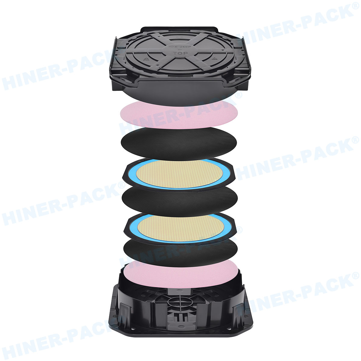
A cassette wafer must satisfy conflicting requirements: rigid mechanical support during transport, yet gentle contact to avoid defect generation. For 300mm fabs, the standard FOUP (Front Opening Unified Pod) follows SEMI E1.9, with slot pitches of 10mm or 12.5mm. However, cassette wafer designs for 200mm often use open cassettes with 6.35mm pitch. Material selection directly impacts particle shedding:
PFA (Perfluoroalkoxy): High chemical resistance, low outgassing – ideal for wet process stations. Coefficient of friction 0.2.
PEEK (Polyether ether ketone): Superior mechanical strength (140 MPa tensile), used in high-temperature applications up to 260°C.
PP (Polypropylene): Cost-effective for 200mm legacy fabs, but limited to <80°C.
ESD-safe composites: Carbon-fiber or conductive polymer blends (surface resistivity 10³–10⁵ Ω/sq) to prevent charge accumulation.
Data from a 2023 industry study showed that replacing standard PP cassettes with PFA-based cassette wafer reduced added particles ≥0.12µm by 78% in copper CMP processes. Hiner-pack offers a full spectrum of wafer carriers made from these materials, each verified for cleanliness to ISO Class 4.
2. Industry Pain Points: Contamination, ESD, and Mechanical Warpage
Semiconductor fabs face three chronic challenges with cassette wafer systems:
Sub-visual particle transfer: Carriers act as reservoirs for particles from previous lots. A single cassette can transfer >2,000 particles (≥0.09µm) to incoming wafers if not properly cleaned.
ESD-induced gate oxide damage: Tribocharging during wafer insertion/extraction can generate voltages exceeding 2kV, enough to rupture 5nm gate oxides. ESD-safe polymers are mandatory for advanced nodes.
Slot deformation and wafer shifting: Repeated thermal cycling (e.g., from 25°C to 150°C in deposition tools) causes warpage in low-grade polymers, leading to wafer edge contact and chipping.
According to SEMI E154, allowable cassette wafer slot pitch variation must stay within ±0.1mm to prevent wafer breakage during robotic handling. Yet many generic carriers exceed this after 500 thermal cycles. This is where precision molding and material stabilization become critical.
3. High-Performance Solutions: Hiner-pack's Precision Cassette Wafer Portfolio
To solve these pain points, Hiner-pack has engineered its cassette wafer series with four proprietary features:
Low-particle PFA molding: Achieves <5 added particles ≥0.1µm per wafer pass (tested per SEMI E46).
Embedded RFID slots: For tracking cassette history (cleaning cycles, lot genealogy) without surface protrusions.
Anti-static dissipation paths: Surface resistivity controlled at 10⁶ Ω/sq, discharging below 50V within 2 seconds.
Thermally stabilized ribs: Maintains slot pitch accuracy within ±0.05mm after 1,000 cycles of 25°C ↔ 120°C.
Beyond the core cassette wafer line, Hiner-pack provides complementary handling tools: JEDEC trays for die sorting, waffle packs for bare die shipping, and gel boxes for fragile MEMS devices. These products share the same contamination control philosophy, ensuring seamless workflow integration.
4. Integration into Automated Material Handling Systems (AMHS)
Modern fabs rely on overhead hoist transport (OHT) and rail-guided vehicles (RGVs). A cassette wafer must feature kinematic coupling plates with repeatability of ±0.2mm for OHT docking. The cassette wafer design also requires:
Compliance with SEMI E15.1 for tool-to-carrier communication.
Weight optimization (≤2.8kg for 25-wafer 300mm FOUP) to reduce OHT motor load.
Vibration damping inserts to keep acceleration-induced wafer movement below 0.3mm.
Field data from a 12-inch fab in Taiwan showed that switching to a precision-balanced cassette wafer reduced OHT alignment errors by 63% and eliminated wafer slippage during high-speed turns (2.5 m/s²).
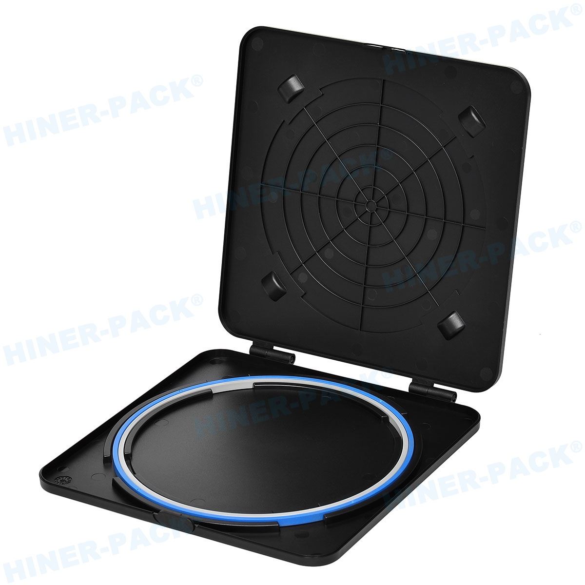
5. Comparative Analysis: Open Cassette vs. FOUP vs. FOSB for Different Process Stages
Not all cassette wafer formats suit every process. A strategic selection matrix based on contamination risk and automation level:
Open Cassette (200mm legacy): Lowest cost, but no environmental isolation. Suitable only for backend assembly where particle control >0.5µm.
FOUP (300mm front-end): Sealed with ISO Class 1 mini-environment, purge ports for N₂/H₂O control. Required for lithography and gate oxidation steps.
FOSB (300mm shipping): Similar seal but without purge; used for inter-fab transport. Must survive 100g shock tests.
For mixed 200mm/300mm fabs, a convertible cassette wafer adapter (e.g., 300mm to 200mm ring) can reduce capital expenditure by 40%. Wafer shipper accessories from Hiner-pack include such adapters with verified particle data.
6. Best Practices for Cassette Wafer Maintenance, Cleaning, and Lifecycle Management
To maximize the usable life of a cassette wafer (typically 2-3 years in high-volume production), follow these protocols:
Cleaning frequency: After every 100 process cycles or when particle monitor exceeds 50 added particles per wafer.
Validated cleaning method: Ultrasonic DI water rinse (18.2 MΩ·cm) with 0.2% non-ionic surfactant, followed by hot air drying (60°C). Avoid IPA—it can stress PFA.
Re-qualification tests: Quarterly measurement of slot pitch, surface resistivity, and particle adders using laser particle counters (LPC).
End-of-life criteria: Slot pitch deviation >0.15mm, surface resistivity drift out of 10³–10⁵ Ω/sq, or visible cracks.
Implementing a cassette tracking system (e.g., barcode or RFID) can reduce misidentification errors by 90% and prevent using a carrier beyond its certified cleanliness level.
The Cassette Wafer as a Yield Enabler
From epitaxy to final test, the cassette wafer is no longer a commodity item. Leading fabs treat it as a process-critical consumable, with specifications reviewed during each technology node transfer. By combining material science (PFA/PEEK), contamination control (SEMI E46), and automation compatibility (SEMI E15.1), engineers can eliminate up to 15% of yield loss attributed to wafer handling. Hiner-pack provides fully documented cassette wafer solutions with material certificates and particle test reports for each batch.
Frequently Asked Questions (FAQ)
Q1: What is the typical particle adder specification for a 300mm cassette wafer used in a 5nm fab?
A1: For sub-10nm nodes, the acceptable particle adder per wafer pass is ≤5 particles ≥0.05µm and ≤1 particle ≥0.1µm, tested according to SEMI E46-0618. Most standard carriers only meet ≥0.1µm control. Hiner-pack offers PFA carriers with certified <2 particles ≥0.05µm.
Q2: Can I reuse a cassette wafer designed for 200mm wafers to handle 150mm wafers?
A2: Not directly. Slot pitch and wafer curvature support differ. However, you can use a precision adapter ring (available from wafer shipper accessories), but verify that the adapter does not raise the wafer's contact point, which could induce edge stress. We recommend dedicated carriers for each diameter.
Q3: How do I measure ESD decay time on a cassette wafer surface?
A3: Use a static decay meter per SEMI E43. Charge the carrier surface to ±1000V, then measure time to drop to ±50V. For ESD-safe carriers, acceptable decay time is <2 seconds at 25% relative humidity. Conductive carriers (10³–10⁵ Ω/sq) typically decay within 0.1 seconds.
Q4: What is the maximum temperature a PFA cassette wafer can withstand without deformation?
A4: PFA carriers can continuously operate at 260°C, making them suitable for post-implant anneal and CVD processes. Short-term spikes up to 300°C are tolerable but may reduce service life. PP carriers are limited to 80°C and should never enter high-temperature furnaces.
Q5: How do I validate a new cassette wafer for my automated wet station?
A5: Run a three-phase test: (1) Dimensional check with a CMM to ensure SEMI E1.9 compliance, (2) Particle adder test by cycling 25 clean monitor wafers through the carrier and measuring added defects, (3) AMHS docking repeatability test using an OHT emulator. Request a validation report from your supplier; Hiner-pack provides this data for all its cassette wafer models.
For technical datasheets, custom cassette wafer designs, or a contamination audit of your current carriers, contact Hiner-pack engineering support: Submit an inquiry with your wafer size, process node, and throughput requirements. A senior applications engineer will respond within 24 hours with recommended specifications and sample test reports.


