
As logic nodes shrink to 3 nm and below, the sensitivity of bare silicon wafers to airborne molecular contamination (AMC) and particles has reached an unprecedented level. A single particle larger than 0.1 µm deposited on a critical die area can render the entire chip worthless. In this zero-defect environment, the choice of wafer carriers directly impacts die yield. OEM wafer box suppliers provide the interface between process tools, automated material handling systems (AMHS), and the wafers themselves. Unlike generic box manufacturers, these suppliers engineer their products to exacting original equipment manufacturer specifications, ensuring dimensional precision, material purity, and long-term reliability. This article examines the technical complexities, application scenarios, and industry challenges that make a strategic partnership with expert suppliers such as Hiner-pack indispensable for modern semiconductor fabs.
Technical Specifications: Beyond Basic Dimensions
An OEM wafer box supplier must guarantee that every pod meets or exceeds SEMI standards while maintaining strict tolerances for automated handling. The following parameters separate commodity boxes from high-performance carriers:
Dimensional Accuracy & SEMI Compliance
Kinematic coupling interface: The three-groove kinematic pin system defined in SEMI E15 and E62 must position the box within ±0.1 mm at the load port. Even slight deviations cause mis-pick by the overhead hoist transport (OHT) or equipment front end module (EFEM).
Wafer pitch and slot numbering: For 300 mm FOUPs, the vertical pitch is exactly 10 mm. OEM wafer box suppliers use precision machining and optical measurement to ensure uniform slot spacing, preventing wafer edge chipping during robotic extraction.
SEMI E100 compliant door latching: The door mechanism must withstand thousands of open/close cycles while maintaining a seal tight enough to maintain nitrogen purge integrity.
Material Science and ESD Control
Bulk material selection is a blend of polycarbonate (PC) or polyetherimide (PEI) blended with carbon nanotubes or carbon fiber to achieve surface resistivity between 10⁴ and 10⁹ Ω/sq – the static dissipative range required to prevent electrostatic discharge damage. Advanced suppliers like Hiner-pack employ compounds that minimize particle shedding and extractable metals. Recent studies show that using an optimized carbon-fiber-reinforced composite can reduce outgassing of volatile organic compounds (VOCs) by up to 40 % compared to standard carbon-filled plastics.
Cleanliness and Outgassing Control
Particle performance: A new FOUP from a qualified OEM wafer box supplier must typically exhibit ≤ 10 particles ≥ 0.1 µm per cubic foot when tested with ultrapure nitrogen.
Outgassing and moisture absorption: The box interior is the immediate microenvironment. Low-moisture-uptake materials prevent the formation of water marks (Haze) on the wafer. Suppliers perform thermal desorption GC-MS to quantify specific organic species that could poison gate oxides.
Critical Applications Across the Semiconductor Value Chain
While front-end fabs are the most demanding users, OEM wafer box suppliers serve multiple nodes across the industry:
Front-Opening Unified Pods (FOUPs) for 300mm Foundries
FOUPs are the workhorses of modern 300 mm fabs. They integrate with load ports that automatically open the door, allowing the EFEM robot to extract individual wafers. OEM specifications dictate features like integrated RFID tags for tracking, purge ports for nitrogen or clean dry air (CDA) injection, and optional humidity sensors. Hiner-pack offers FOUPs with a patented multi-stage purge diffuser that reduces oxygen concentration inside the pod to below 100 ppm within 60 seconds, protecting copper interconnects from oxidation.
FOSBs for Shipping and Inter-Fab Transport
Front-Opening Shipping Boxes (FOSBs) are designed to protect wafers during transit between fabs or to outsourced assembly and test (OSAT) facilities. Unlike FOUPs, they are usually sealed with a screw or latch and may not be purged. However, they still require the same dimensional precision to avoid damage from vibration. OEM-grade FOSBs incorporate shock-absorbing wafer cushions and are molded from materials that pass ISTA 2A transport tests.
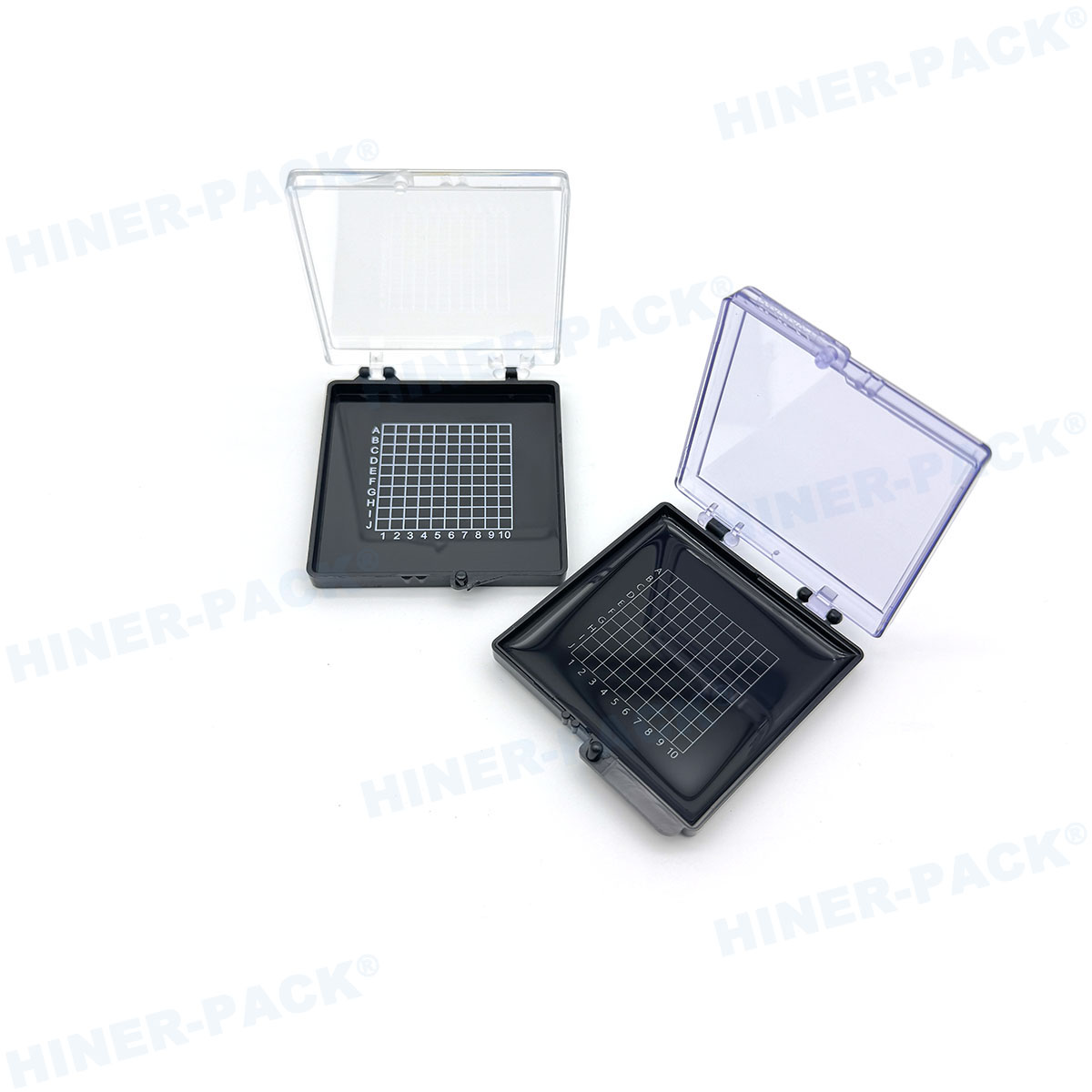
Custom Reticle Pods and SMIF Pods
Although 300 mm dominates, 200 mm fabs still rely on Standard Mechanical Interface (SMIF) pods. Additionally, extreme ultraviolet (EUV) lithography requires ultra-clean reticle pods that protect photomasks from any haze-forming contaminants. OEM wafer box suppliers extend their expertise to these specialized carriers, often using multi-layer materials to shield against actinic light and particles.
Industry Pain Points and Supplier-Driven Solutions
Fabs constantly face operational issues that can be traced back to wafer boxes. Here is how top OEM wafer box suppliers address these challenges:
Particle Adders and Cross-Contamination
Pain point: Over time, boxes accumulate particles from process residuals (e.g., CMP slurry, dielectric etch by-products). These particles can transfer to wafers during subsequent handling.
Solution: Premium suppliers now offer smooth, non-porous interior surfaces and rounded corners that are easy to clean. Some, including Hiner-pack, apply a permanent anti-adhesion coating that reduces particle adhesion force, making ultrasonic cleaning more effective.
Moisture and Oxygen Ingress
Pain point: Moisture absorbed in the box walls slowly releases inside the pod, causing native oxide growth or corrosion of sensitive metals (e.g., cobalt, ruthenium).
Solution: Use of low-water-absorption resins combined with active purge systems. Advanced boxes feature integrated valves that mate with factory purge nozzles, enabling fast, repeatable purging cycles.
RFID Communication Failures
Pain point: Metal-rich plastics can detune or block RFID signals, leading to read failures at the load port.
Solution: Expert suppliers precisely control the filler concentration and design recessed pockets for RFID inlays, ensuring reliable communication without compromising ESD properties.
Evaluation Criteria for Selecting an OEM Wafer Box Supplier
When qualifying a new partner, fab engineers should consider these five technical pillars:
Cleanroom manufacturing: Does the supplier mold and assemble in at least ISO Class 5 (Class 100) cleanrooms? Secondary operations should also be performed in a controlled environment to avoid particle entrapment.
Traceability and serialization: Every box should have a laser-marked 2D barcode that links to manufacturing data – material lot, molding tool cavity, and date code.
Metrology capabilities: The supplier must provide dimensional measurement reports using coordinate measuring machines (CMM) with sub-micron accuracy.
Material certification: Request outgassing test data per SEMI F30 and extractable metal analysis (ICP-MS).
Customization lead time: Can they modify the wafer cushion design or integrate a customer-specific RFID tag without requalifying the entire box?
Only OEM wafer box suppliers that operate their own in-house testing laboratories and employ materials scientists can consistently meet these criteria.
Case in Point: Hiner-pack’s Contribution to Advanced Fabs
Hiner-pack has established itself as a trusted partner for several tier‑1 logic and memory manufacturers. Their 300 mm FOUPs are engineered with a proprietary conductive polycarbonate blend that achieves a surface resistance of 10⁶ Ω, eliminating the need for a separate grounding clip. Field data from a 5 nm fab showed a 30 % reduction in incoming particle counts after switching to Hiner-pack’s fifth‑generation FOUP. Furthermore, the company offers a rapid customization service: they recently delivered a batch of anti‑static FOSBs with a modified door latch to accommodate an automated screw‑driving station at a major OSAT, all within four weeks. Such agility, combined with full SEMI compliance, exemplifies why OEM wafer box suppliers like Hiner-pack are becoming integral to yield improvement roadmaps.
Future Trends: 450mm Transition and Smart Pods
Although 450 mm wafer adoption has slowed, the development work has pushed the boundaries of box technology. Future boxes will likely incorporate sensors for real‑time monitoring of humidity, oxygen, and particle counts – the “smart pod” concept. OEM wafer box suppliers are already experimenting with embedding low‑power MEMS sensors that communicate via near‑field communication (NFC) to the fab’s host system. Additionally, as EUV lithography moves to high‑volume manufacturing, the need for hydrogen‑compatible boxes (to mitigate tin debris from the source) will create new material challenges. Suppliers with deep R&D resources will lead this innovation.
Frequently Asked Questions
Q1: What exactly does an OEM wafer box supplier do that differentiates them from standard box manufacturers?
A1: An OEM wafer box supplier designs and manufactures wafer carriers that meet the exact specifications of semiconductor equipment and fab automation systems. They ensure strict adherence to SEMI standards, provide full material traceability, and often collaborate with fabs to optimize carrier design for specific processes, such as high‑temperature bakes or vacuum compatibility.
Q2: How do I verify if a supplier meets my required OEM specifications?
A2: Request a detailed qualification report including dimensional measurements (using a CMM), surface resistivity mapping, particle shedding tests, and outgassing analysis (GC‑MS). A reliable supplier like Hiner-pack will also provide a certificate of conformance linking each box to its production batch.
Q3: Can OEM wafer boxes be customized for older 200 mm fabs with non‑standard load ports?
A3: Yes. Many OEM wafer box suppliers offer engineering services to adapt SMIF pod designs or create adapter plates for legacy equipment. Customization may involve adjusting the kinematic coupling location or modifying the door latch to match manual load ports.
Q4: What is the typical lead time for a batch of OEM‑grade FOUPs from a supplier like Hiner-pack?
A4: For standard products, lead times usually range from 4 to 8 weeks, depending on the quantity and material availability. Customized designs with new mold inserts may require 12–16 weeks for tooling and validation. Hiner-pack offers expedited sampling for critical applications.
Q5: How often should wafer boxes be cleaned or replaced in a high‑volume fab?
A5: Cleaning frequency depends on the process environment. Typically, FOUPs are cleaned every 20–30 cycles in a Cu/low‑k fab, while less critical areas may clean every 60 cycles. Replacement is recommended when the box shows signs of wear (e.g., chipping on the door plate) or when particle counts cannot be reduced below spec after repeated cleaning. Hiner-pack provides guidelines based on cumulative usage hours.
Q6: Are there specific SEMI standards that govern wafer box manufacturing?
A6: Yes. Key standards include SEMI E15 (Specification for 300 mm Load Port), SEMI E62 (FOUP interface), SEMI E100 (FOUP door), and SEMI F30 (Test method for outgassing). Suppliers should also follow SEMI S2 for safety and SEMI E176 for RFID on carriers.


