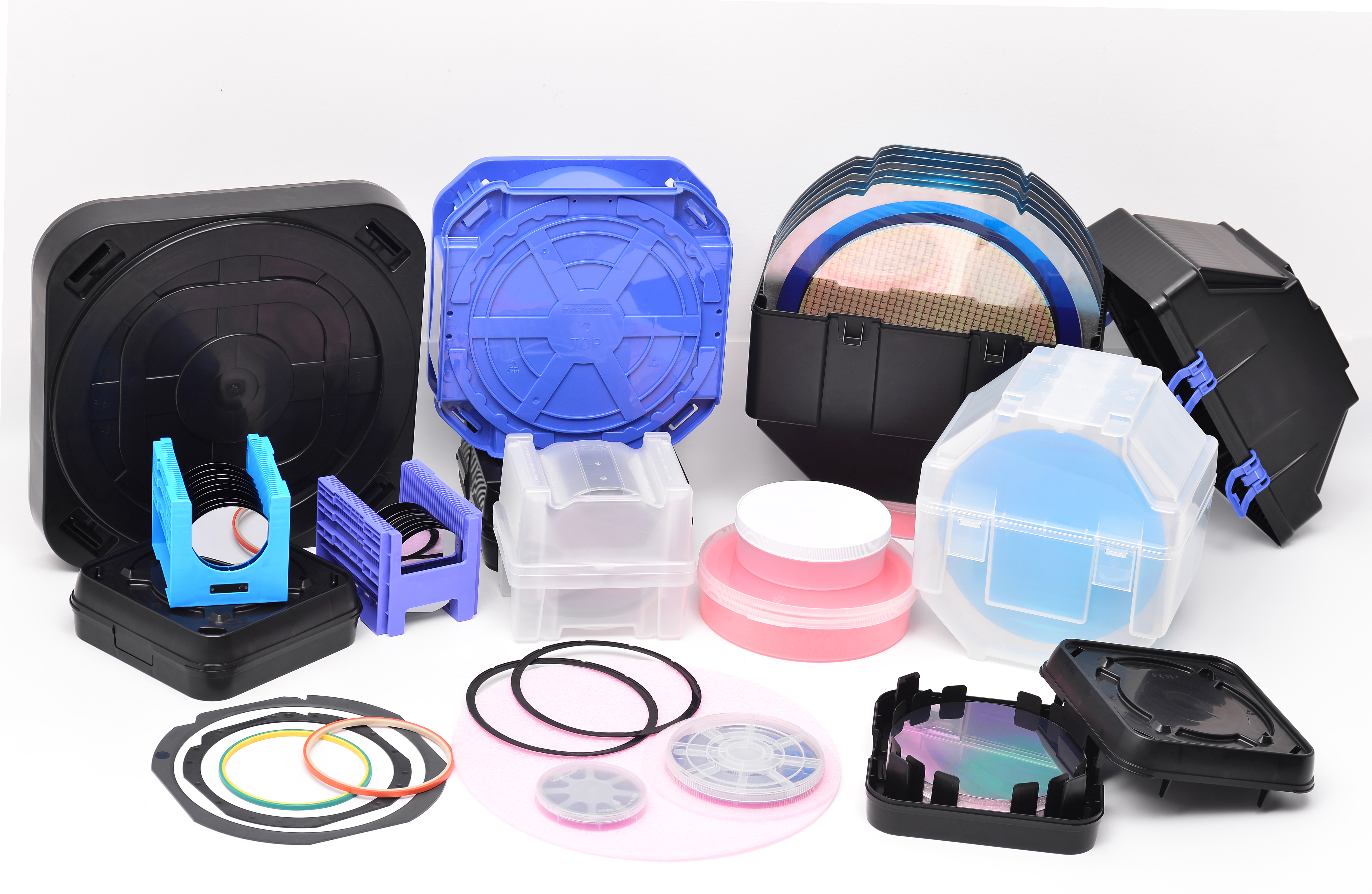
In the high-stakes world of semiconductor manufacturing, every nanometer counts. Protecting delicate silicon wafers from contamination, physical damage, and electrostatic discharge (ESD) is not just a logistical step; it’s a fundamental requirement for maintaining yield. At the heart of this protection are wafer storage boxes, also commonly referred to as wafer carriers or cassettes. Choosing the right box is a direct investment in product integrity. Companies like Hiner-pack have dedicated engineering efforts to meet these precise needs with robust and reliable solutions.
Why the Right Wafer Storage Box is Non-Negotiable
A wafer storage box is far more than a simple container. It is a precision-engineered ecosystem designed to cradle and shield wafers worth thousands of dollars through various stages—from post-fabrication and metrology to shipping and intermediate storage. A single particle or an unnoticed static event can render a wafer useless, leading to significant financial loss.
The primary mission of any semiconductor wafer storage box is to provide a secure, clean, and stable environment. This demands excellence in material science, design fidelity, and compliance with international industry standards.
Key Considerations When Selecting a Wafer Storage Box
Material and Chemical Resistance
The construction material is paramount. High-purity polycarbonate (PC) and polypropylene (PP) are industry staples. These materials must be inherently clean, low-outgassing, and resistant to chemicals used in fabrication, such as solvents and acids. The material must also withstand repeated cleaning cycles without degrading or becoming brittle.
A premium wafer storage box will often incorporate additives for static control without compromising chemical purity. This ensures no leachable contaminants come into contact with the wafer surface.
ESD Protection and Contamination Control
Electrostatic discharge is a silent killer of microelectronics. Conductive or dissipative wafer storage boxes are essential to safely ground any static charge, preventing catastrophic damage to integrated circuits. The box material must have a consistent surface resistivity within safe ranges (e.g., 10^4 to 10^11 ohms/sq).
Furthermore, design features like secure, latching lids and integrated sealing surfaces are critical. They prevent ambient airborne particles, which are abundant in any environment, from settling on the wafers. Some advanced designs from providers like Hiner-pack include labyrinth seals or gaskets for an extra layer of protection in challenging environments.
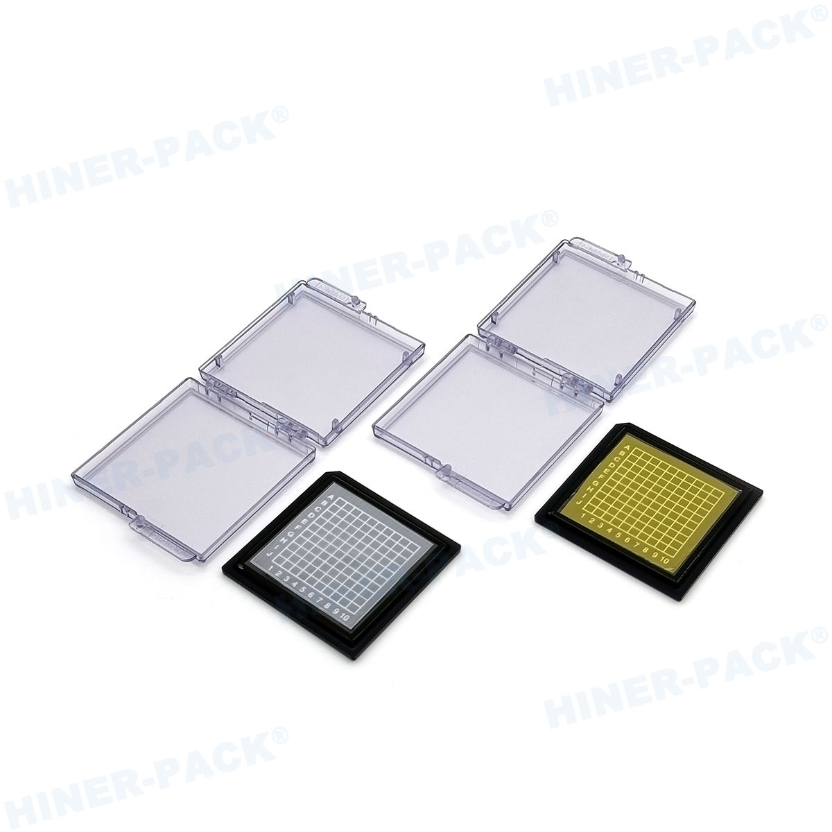
Capacity, Dimensions, and Compliance
Standardization is key for automation. Wafer storage boxes must comply with SEMI standards (e.g., SEMI E1.2, E15.1, E62) for dimensions and capacity. Common capacities are 25 wafers for 200mm and 300mm sizes, and 13 wafers for 450mm. The box must interface flawlessly with automated Material Handling Systems (AMHS), robotic arms, and processing tools.
Precision-molded slots maintain exact wafer pitch, preventing contact between wafers and minimizing vibration during transport. This prevents edge chipping and surface abrasion.
Mechanical Strength and Stackability
In a busy fab, wafer storage boxes are handled frequently and may be stacked to save cleanroom floor space. The structure must have excellent mechanical rigidity to prevent warping under load. Reinforced corners and interlocking stackability features are vital. A stack of boxes filled with wafers is heavy; the bottom box must bear the weight without deformation.
Thermal and Vacuum Compatibility
For certain processes, boxes may need to withstand brief exposure to elevated temperatures or vacuum environments. The material must not deform or release gases (outgas) under these conditions, which could contaminate a process chamber or the wafers themselves.
The Total Cost of Ownership: Beyond the Purchase Price
While upfront cost is a factor, the true cost of a wafer storage box is measured over its lifespan. A durable box that withstands thousands of cleaning cycles, maintains its ESD properties, and protects wafers through millions of robotic transfers offers a far better return on investment than a cheaper, less robust alternative.
Reduced particle generation, lower wafer breakage rates, and seamless automation compatibility all contribute to higher overall equipment effectiveness (OEE). This is where partnering with an experienced manufacturer proves invaluable. Hiner-pack, for instance, focuses on engineering for longevity and reliability, directly impacting a fab’s bottom line by safeguarding yield.
Applications Beyond Simple Storage
Modern wafer storage boxes are integrated into larger systems. They are used in:
•SMIF (Standard Mechanical Interface) Pods: Creating a mini-environment.
•FOUP (Front-Opening Unified Pod) & FOSB (Front-Opening Shipping Box): Essential for 300mm wafer automation and inter-facility transport.
•Shipping and Logistics: Heavy-duty, certified containers designed to protect wafers across global supply chains against shock, vibration, and pressure changes.
Looking Ahead: Smarter Storage Solutions
The future points towards “smart” carriers. Integration with RFID tags for wafer-level tracking and data logging for environmental conditions (temperature, humidity, shock) are becoming more prevalent. The fundamental wafer storage box, however, remains the indispensable physical layer upon which these smart systems are built.
Selecting the optimal wafer storage box requires a careful balance of material properties, mechanical design, and standards compliance. It is a critical component link in the semiconductor manufacturing chain, where the cost of failure is exceptionally high. Investing in high-quality carriers from trusted suppliers is a straightforward strategy to mitigate risk and protect valuable product.
Frequently Asked Questions (FAQs)
Q1: What is the difference between a conductive and a dissipative wafer storage box?
A1: Conductive wafer storage boxes have very low surface resistivity (typically 10^4 to 10^6 ohms/sq), allowing charge to ground very quickly. Dissipative boxes have higher resistivity (10^7 to 10^11 ohms/sq), allowing charge to drain safely but more slowly, preventing rapid discharge (sparks). The choice depends on the specific sensitivity of the wafers and the factory’s ESD control protocol.
Q2: How often should wafer storage boxes be cleaned, and what method is recommended?
A2: Cleaning frequency depends on the cleanroom class and usage. Boxes moving between less clean areas may need cleaning every cycle. Standard practice involves using dedicated DI water (Deionized water) systems, sometimes with mild, semiconductor-grade detergents, followed by thorough drying in a particle-controlled environment. Ultrasonic baths are also common. Always follow the manufacturer’s guidelines, such as those provided by Hiner-pack, to avoid material degradation.
Q3: Can I use the same box for 200mm and 300mm wafers?
A3: No. Wafer storage boxes are precision-molded for specific wafer diameters. Using an incorrect size will not provide proper support, leading to a high risk of wafer slipping, contact, breakage, and failure in automated handling systems. Always use the box designed for your exact wafer size.
Q4: What SEMI standards are most relevant for wafer storage boxes?
A4: Key standards include SEMI E1.2 for 300mm mechanical handling, SEMI E15.1 for 200mm boxes, and SEMI E62 for carrier mechanical specifications. For shipping, SEMI E47 and E1.9 are crucial. Compliance ensures interoperability with global semiconductor equipment.
Q5: Why might a manufacturer like Hiner-pack emphasize specific polymer grades in their boxes?
A5: Not all polycarbonate or polypropylene is equal. Semiconductor-grade polymers have ultra-low levels of ionic and metallic impurities, minimal outgassing potential, and consistent lot-to-lot quality. A manufacturer like Hiner-pack selects and tests these high-purity resins to ensure their wafer storage boxes do not become a source of contamination, thereby directly protecting the customer’s process yield.


