
In semiconductor manufacturing steps such as chemical mechanical planarization (CMP), wet cleaning, spin rinsing, and metrology inspection, the wafer grip ring (also known as a wafer clamp ring or retaining ring) is a critical consumable that directly affects wafer flatness, edge exclusion, and defectivity. A poorly designed grip ring leads to wafer slippage, uneven film removal, edge chipping, and particle generation. Hiner-pack has engineered precision grip rings for over a decade, serving leading IDMs and wafer foundries with materials optimized for acidic slurries, high-velocity rinsing, and automated wafer handling. This article details the engineering parameters that define a reliable wafer grip ring for 200mm and 300mm processing.
1. Core Functions of a Wafer Grip Ring in Semiconductor Equipment
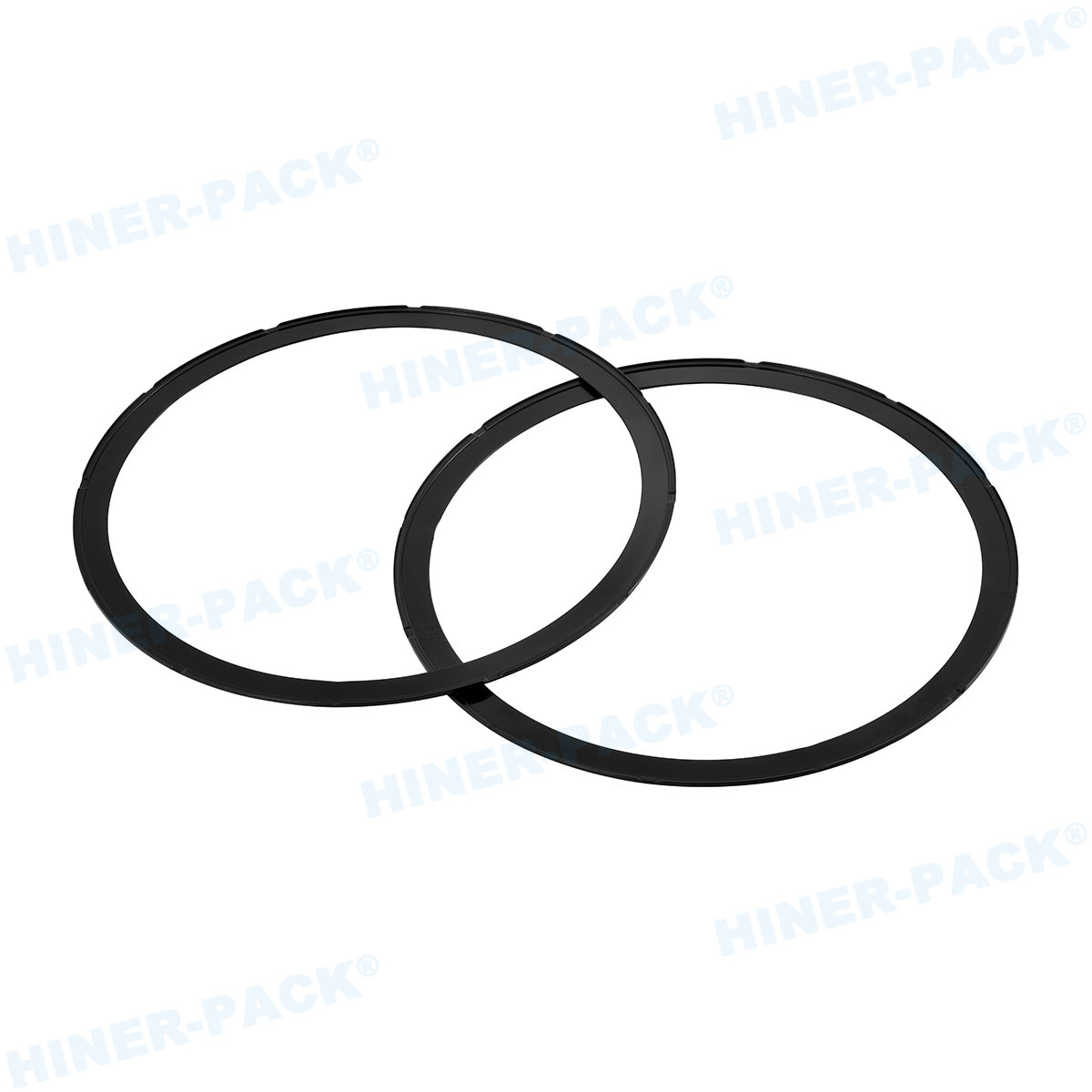
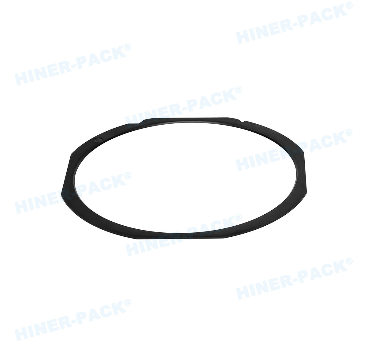
The wafer grip ring is a circular clamping device that secures the wafer to a rotating chuck or a stationary platen during processing. Its primary roles include:
Clamping force distribution: Applies uniform downward pressure on the wafer edge to prevent movement during high-speed rotation (up to 2000 rpm in CMP or spin cleaners).
Edge exclusion management: Shields the outermost 2–5 mm of the wafer from processing, preventing edge bead formation or slurry ingress.
Chemical and mechanical isolation: Protects the chuck from abrasive slurries (CMP) or aggressive chemistries (SC1, SC2, DHF).
Wafer centering and alignment: Mechanical features (pins, chamfers) ensure repeatable wafer positioning across multiple tools.
Particle and metallic contamination control: Materials must resist corrosion and minimize shedding of particles >0.1 µm.
In CMP applications, the grip ring also acts as a retaining ring, preventing the wafer from slipping out from under the polishing head. Hiner-pack's grip rings are validated to maintain clamping force within ±5% over 10,000 cycles without permanent deformation.
2. Material Selection: PEEK, PPS, PVDF, and Ceramic Options
The choice of wafer grip ring material depends on the chemical environment, temperature, and mechanical stress. Four material families dominate the market:
PEEK (polyether ether ketone): Most widely used for CMP retaining rings and wet etch clamps. Offers excellent chemical resistance (pH 1–14 except concentrated sulfuric acid), high flexural modulus (18 GPa), and continuous use temperature up to 260°C. PEEK grip rings from Hiner-pack are glass-filled (30%) to improve wear resistance against abrasive slurries. Preferred for copper CMP and STI CMP.
PPS (polyphenylene sulfide): Lower cost than PEEK, with good chemical resistance but lower mechanical strength (flexural modulus 12 GPa). Maximum operating temperature 200°C. Suitable for less abrasive processes (post-CMP cleaning, spin drying). However, PPS is more brittle and may crack under repeated clamping cycles. Hiner-pack offers PPS rings for non-critical, low-volume applications.
PVDF (polyvinylidene fluoride): Excellent resistance to ozone and oxidizing chemistries (e.g., SPM, H₂O₂). Used in wet benches for wafer cleaning. PVDF has lower stiffness (8 GPa) and requires thicker cross-sections. Not recommended for high-clamping-force applications.
Ceramic (alumina or zirconia): Ultra-high hardness (15 GPa) and wear resistance, zero particle shedding. Used in tungsten CMP or other aggressive planarization steps where polymer rings wear out quickly. However, ceramics are expensive and can damage wafer edges if misaligned. Hiner-pack supplies ceramic rings only for customers with proven handling protocols.
For most 300mm CMP applications, PEEK with 30% carbon fiber reinforcement provides the best balance. Hiner-pack's wafer handling accessories product line includes PEEK grip rings with laser-etched batch traceability.
3. Critical Dimensional and Mechanical Specifications
A wafer grip ring must conform to equipment-specific dimensions and clamping force requirements. Key parameters include:
Outer diameter (OD): Matches the chuck or polishing head receiver. For 300mm CMP heads, typical OD = 310–320 mm. For 200mm tools, OD = 220–230 mm. Tolerance ±0.05 mm to ensure proper seating.
Inner diameter (ID): Determines edge exclusion zone. For a 300mm wafer, ID = 296–298 mm (exclusion 1–2 mm). A larger ID reduces wafer contact but allows more slurry undercutting. Hiner-pack provides ID from 290 mm (aggressive exclusion) to 298 mm (minimal exclusion).
Thickness: Typically 5–15 mm depending on the tool. Thicker rings provide higher clamping force rigidity but increase head mass. Variation across the ring must be <0.03 mm to prevent uneven pressure.
Flatness and parallelism: The bottom surface (contacting the chuck) must have flatness ≤0.02 mm. Parallelism between top and bottom surfaces ≤0.03 mm. Measured on a granite plate with a dial indicator.
Clamping force uniformity: Measured using pressure-sensitive film (Fuji Prescale). The ring should exert 20–50 N per linear cm of circumference with variation <±10%. Hiner-pack tests every batch of grip rings using a custom force-mapping fixture.
Surface roughness (Ra): The wafer contact surface should be ≤0.8 µm to avoid scratching the wafer backside. The chuck-facing surface can be rougher (Ra 1.6–3.2 µm) to prevent vacuum leakage.
Hiner-pack provides a dimensional inspection report with each grip ring, including CMM measurements of ID, OD, thickness, and flatness.
4. Surface Finish and Cleanroom Compatibility
Particle generation from the grip ring is a major source of killer defects (particles >0.2 µm) on the wafer backside and edge. The surface finish must balance low friction with low shedding.
For PEEK and PPS rings: Injection molding with polished cavities produces Ra ≤0.4 µm without secondary machining. However, mold flash must be removed by cryogenic deflashing or hand trimming. Hiner-pack uses a CO₂ snow jet cleaning to remove particles and static charge. Outgassing per SEMI F57-1112 is below 0.1 µg/g for VOCs.
For ceramic rings: Grinding and lapping to Ra ≤0.2 µm, followed by ultrasonic cleaning in DI water and IPA. No organic residues allowed.
ESD control: Surface resistivity should be between 10⁵ and 10¹¹ Ω/sq to prevent static attraction of particles. PEEK rings are compounded with carbon nanotubes (CNT) to achieve 10⁶–10⁸ Ω/sq. Hiner-pack measures resistivity per SEMI E129.
Metal ion contamination: Inductively coupled plasma mass spectrometry (ICP-MS) analysis ensures that extractable metals (Na, Fe, Cu, etc.) are below 1 ppb per SEMI F40. Hiner-pack's PEEK rings meet the requirements for copper barrier and gate oxide processes.
For fabs running 5nm and below nodes, Hiner-pack offers an “ultra-clean” version of the grip ring with double vacuum bagging and argon purge packaging to maintain cleanliness below 10 particles >0.1 µm per ring.
5. Compatibility with Processing Chemistries and Slurries
The wafer grip ring must survive thousands of cycles of exposure to aggressive chemicals. Below are common chemistries and material compatibility:
Oxide CMP slurries (silica-based, pH 10–11): PEEK and PPS are both resistant. However, silica particles can mechanically wear PPS faster. Hiner-pack recommends carbon-filled PEEK for oxide CMP to reduce wear rate.
Tungsten CMP slurries (alumina or silica, pH 2–4): Acidic conditions attack PPS and some grades of PEEK. Hiner-pack uses a special PEEK formulation with enhanced acid resistance (no hydrolysis).
Copper CMP slurries (pH 3–5 with benzotriazole): No material issues for PEEK. However, copper ions can plate onto ceramic rings – not recommended.
Post-CMP cleaning (SC1: NH₄OH/H₂O₂, 60–80°C): PEEK is fully resistant. PVDF also works but has lower temperature limit (100°C). PPS degrades in hot SC1.
HF-based etchants (DHF, BHF): PEEK is resistant up to 48% HF at room temperature. PPS and PVDF are not recommended for HF.
SPM (H₂SO₄/H₂O₂, 120–150°C): Only PEEK and ceramic survive. PPS and PVDF decompose.
Hiner-pack provides a chemical compatibility chart with each grip ring order, based on the customer’s specified process chemicals.
6. Industry Pain Points and Engineering Solutions
6.1 Uneven Clamping Force Causing Wafer Edge Cracks
Problem: Injection-molded PEEK rings can have residual
stresses that cause warpage after repeated thermal cycles (e.g., from hot SC1
cleaning to room temperature). Warpage reduces clamping force on one side of the
wafer, leading to edge chipping or wafer breakage.
Solution: Hiner-pack anneals all PEEK grip rings at 200°C for 4 hours after molding,
followed by slow cooling (10°C/hour). This relieves internal stresses and
stabilizes flatness. Post-annealing flatness is ≤0.02 mm across the ring. We
also add a 0.5 mm compliant silicone pad on the clamping surface to compensate
for minor chuck irregularities.
6.2 Abrasive Slurry Trapping and Particle Generation
Problem: Grip rings with sharp corners or rough surfaces
trap abrasive slurry particles. During the next wafer cycle, these particles
dislodge and scratch the wafer backside or edge.
Solution: Hiner-pack designs all grip rings with a 15° chamfer on all edges and a smooth
transition between the clamping surface and the outer wall. The surface is
polished to Ra ≤0.4 µm. Additionally, we incorporate a spiral groove on the
chuck-facing side to allow slurry or cleaning fluid to escape, preventing
particle buildup. This design reduces particle adders by 70% compared to
conventional flat rings.
Problem: In fabs with multiple CMP tools and cleaning
stations, tracking grip ring usage (cycles, chemical exposure, wear) is manual
and error-prone. Worn rings cause process drift. Client: A 300mm logic fab in Korea producing 14nm
devices. Q1: What is the typical lifetime of a PEEK wafer grip ring in
CMP? Q2: Can I recondition or regrind a worn grip ring? Q3: How do I prevent vacuum leakage between the grip ring and the
chuck? Q4: What is the maximum rotation speed for a wafer grip ring in spin
cleaning? Q5: How do I clean a wafer grip ring between batches to avoid
cross-contamination? Q6: What is the typical lead time for a custom-sized wafer grip
ring? Q7: Do you provide grip rings with alignment pins or anti-rotation
features? The wafer grip
ring is a consumable that directly impacts CMP uniformity, defect
density, and tool uptime. Hiner-pack provides material
selection guidance, custom molding, and DLC coating services. Our engineering
team can simulate clamping force distribution using FEA and recommend the
optimal material (PEEK, PPS, or ceramic) based on your slurry chemistry,
rotation speed, and temperature profile. Request a quote or sample kit today: Send your wafer size
(200mm or 300mm), tool make/model (e.g., Applied Materials Mirra, Ebara F-REX,
Lam Teres), and annual usage. We will respond within 24 hours with dimensional
drawings, material data sheets, and pricing.
Solution: Hiner-pack embeds a 13.56 MHz RFID tag (ISO 15693) into a recessed pocket on the
ring’s outer rim. The tag withstands 150°C and all common chemistries. Each ring
is pre-encoded with a unique ID, manufacturing date, and material lot number.
When mounted on the tool, an RFID reader records the ring ID, and the tool’s
software tracks cumulative cycles. The system alerts maintenance when the ring
reaches its end-of-life (e.g., 10,000 cycles). This reduces unplanned downtime
and improves CMP uniformity.7. Real-World Case: Extending Grip Ring Lifetime in Copper CMP
Problem: Standard PEEK grip rings wore out after
6,000 wafers, causing non-uniform removal rates and edge over-polishing. The
frequent replacement cost $1,200 per ring and 2 hours of tool downtime each
time.
Solution: Hiner-pack supplied carbon-fiber-reinforced
PEEK grip rings with a diamond-like carbon (DLC) coating on the slurry-facing
surfaces. The DLC coating (2 µm thick) reduced abrasive wear by a factor of 5.
Additionally, the ring’s inner diameter was increased from 296 mm to 297.5 mm to
reduce edge pressure.
Result: The new wafer grip
ring lasted 28,000 wafers, a 4.7x improvement. Tool downtime for
ring changes dropped from 2 hours every 6,000 wafers to 2 hours every 28,000
wafers. Annual savings exceeded $90,000 per tool. The fab standardized on
Hiner-pack’s DLC-coated rings across all 12 CMP tools.Frequently Asked Questions (FAQs) about Wafer Grip Rings
A1: In oxide CMP with silica slurry, a standard unfilled PEEK
ring lasts 8,000–12,000 wafer passes. In copper CMP (more abrasive), lifetime is
4,000–6,000 passes. With carbon fiber reinforcement and DLC coating, lifetime
extends to 20,000–30,000 passes. Hiner-pack provides wear rate data based on
your specific slurry chemistry.
A2:
Yes, for PEEK and PPS rings, regrinding the wafer contact surface can restore
flatness if wear depth is <0.2 mm. Hiner-pack offers a regrinding service for
$25–40 per ring (depending on size) with a 1-week turnaround. Ceramic rings are
not reconditionable due to risk of micro-cracking. We recommend replacement
after regrinding twice, as the ring becomes thinner and may flex.
A3: Ensure the chuck-facing surface of the ring has a spiral
or radial groove pattern (0.3 mm deep, 1 mm wide) to allow air to escape.
Hiner-pack’s rings include a “vacuum relief” groove. Also, verify that the
chuck’s O-ring is not damaged. If leakage persists, apply a thin film of vacuum
grease (Fomblin) compatible with semiconductor processing.
A4: For a 300mm wafer with a PEEK grip ring, the maximum
safe speed is 2,000 rpm (centrifugal force ≈ 500 N on the ring). Above that, the
ring may lift off the chuck or cause wafer slippage. Hiner-pack’s rings are
dynamically balanced to <0.1 g·mm to minimize vibration. For high-speed
applications (3,000+ rpm), we recommend a ring with a locking mechanism (bayonet
or screw mount).
A5: Standard cleaning protocol: 1) Rinse with
deionized water to remove bulk slurry; 2) Ultrasonic clean in 2% non-ionic
surfactant at 50°C for 15 minutes; 3) Rinse with DI water; 4) Ultrasonic in IPA
for 10 minutes; 5) Dry with filtered nitrogen. For metal ion-sensitive
processes, add a 5-minute dip in 1% HF followed by DI rinse. Hiner-pack provides
a cleaning validation kit with particle coupons.
A6: For standard 200mm and 300mm rings with PEEK material,
lead time is 2–3 weeks for quantities up to 100 pieces. For custom IDs,
thicknesses, or material (ceramic), lead time is 5–6 weeks including injection
molding tooling. Hiner-pack maintains inventory of the most common 300mm PEEK
rings (297 mm ID, 10 mm thickness) for 3-day emergency shipment.
A7: Yes. Hiner-pack can integrate stainless steel or PEEK
alignment pins (2 or 3 pins) into the ring’s outer diameter to mate with
matching slots in the chuck. We also offer a keyway or flat orientation feature.
These options add 2–3 days to lead time. For automated wafer handling, we
recommend RFID + pin alignment.Ready to Optimize Your Wafer Grip Ring Performance?


