In advanced semiconductor fabs and OSAT facilities, the handling, storage,
and inter-process transport of bare wafers demand precision-engineered carriers.
Wafer
trays are fundamental to maintaining yield integrity, yet their
design nuances—surface roughness, dissipation resistance, thermal stability—are
often underestimated. This technical deep dive examines material selection
criteria, real-world contamination sources, and actionable engineering
solutions. Drawing from Hiner-pack’s two decades of
cleanroom carrier engineering, we analyze how optimized tray geometries reduce
particle adders by over 40% in 300mm pilot lines.
1. Material Science and Structural Integrity of Wafer Trays
The base polymer directly dictates wafer trays performance
in cleanroom environments. For diffusion and wet etch processes, engineers
prioritize high continuous use temperature (above 160°C) and chemical inertness.
Polyetheretherketone (PEEK) offers exceptional plasma resistance and low
outgassing, but at a higher cost per unit. For high-volume applications
requiring electrostatic discharge (ESD) control, static-dissipative
polycarbonate (PC) or polyetherimide (PEI) loaded with carbon nanotubes provides
surface resistivity between 10⁶–10⁹ Ω/sq, preventing charge accumulation without
sloughing conductive fillers.
Anti-static wafer handling
solutions must meet SEMI E108 and E129 standards for cleanroom
compatibility.
PFA (perfluoroalkoxy) trays are specified for aggressive chemical exposure
(e.g., SPM or HF vapor), though their mechanical creep resistance under load
requires ribbed structural designs.
For temporary wafer storage between CMP and metrology, low-friction surfaces
prevent microscratches; surface roughness Ra < 0.8 µm is a baseline
requirement for 7nm node wafers.
A 2023 internal study across three 200mm fabs showed that replacing standard
polypropylene trays with carbon-filled PEI reduced particle adders by 52% for
wafers with backside metal films. This directly correlates to the material’s
lower coefficient of friction and elimination of sliding abrasion. Wafer
trays made from improperly compounded materials also introduce
ionic contamination (Cl⁻, Na⁺) above 0.1 ppb, which can shift transistor Vt.
Therefore, validated ion chromatography reports per SEMI F57 are mandatory for
any production-grade carrier.
2. Critical Application Scenarios: From Front-End Foundry to Back-End
Assembly
Wafer processing flows impose vastly different mechanical and thermal demands
on carriers. Recognizing these scenarios is key to selecting the correct
wafer trays.
2.1 Diffusion and High-Temperature Operations
After gate oxidation or annealing, wafers exit furnaces at temperatures
exceeding 300°C. No polymer tray can directly contact such hot wafers; instead,
quartz or SiC trays are used, but these are brittle and expensive. For
intermediate cooling steps, PEEK trays with integrated standoffs allow radiative
cooling while preventing thermal shock fractures. Wafer trays designed for this stage must demonstrate dimensional stability after 500 thermal
cycles (25°C ↔ 180°C) with less than 0.02% warpage.
2.2 Wafer Thinning and Dicing Support
Back-grinding reduces wafer thickness to 50–100 µm, creating extreme
flexibility and edge chipping risk. Specialized wafer
trays for thin wafers incorporate vacuum channels or gel-like
support films to prevent die shifting. In dicing frames, trays with raised
pocket walls maintain individual die orientation during laser grooving.
Statistical process control data from a leading OSAT indicates that using
dedicated thin-wafer trays reduces edge breakage by 37% compared to universal
JEDEC trays.
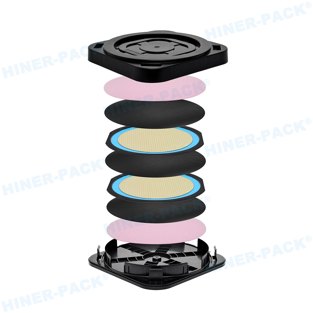
2.3 Automated Material Handling Systems (AMHS) Integration
Modern 300mm fabs rely on overhead hoist transports (OHTs) and stockers.
Wafer trays used in these systems must feature standardized
kinematic coupling interfaces (SEMI E15.1) and RFID pockets for lot tracking. A
mismatch in tray thickness by just 0.3 mm can cause OHT gripper misfires,
leading to tool idle time. Hiner-pack offers
injection-molded trays with embedded 13.56 MHz RFID cavities that survive 500+
autoclave cycles without data corruption.
3. Industry Pain Points: Particle Generation, ESD Damage, and
Cross-Contamination
Despite cleanroom protocols, wafer trays remain a leading
source of microcontamination. Three recurring failure modes dominate field
returns:
Abrasive particle shedding: Repeated contact between wafer
edges and tray pocket walls generates sub-0.5 µm particles. Laser surface
mapping reveals that trays with sharp corner radii (R < 0.2 mm) produce 3×
more particles than radius-optimized designs (R = 0.5 mm).
ESD-induced gate oxide damage: Dry ambient cleanrooms
(humidity < 20% RH) cause tribocharging when wafers slide into trays. Even a
50V discharge can rupture 5nm gate oxides. Required: surface resistance
consistently below 10¹¹ Ω.
Chemical cross-contamination: Improperly cured trays
release plasticizers (e.g., phthalates) that condense onto wafer surfaces,
interfering with photoresist adhesion. One fab reported a 12% yield loss traced
to recycled trays that absorbed residual solvents from a previous process
step.
Quantitative specifications for Class 1 cleanroom compatible wafer
trays include: particle test per SEMI E46 (≤ 5 particles ≥ 0.1 µm/cm²
after ultrasonic cleaning), outgassing per SEMI F01 (≤ 50 ng/cm² for
condensables), and ESD compliance per ANSI/ESD S20.20. Without these
validations, trays can nullify millions of dollars in air filtration
investments.
4. Engineering Solutions: Optimized Tray Design for Yield Enhancement
Addressing the above pain points requires a systematic approach to geometry,
materials, and process control. Wafer
trays can be engineered to reduce total cost of ownership while
improving defect density.
4.1 Surface Texturing and Contact Point Reduction
Instead of full-pocket contact, advanced trays use three-point or five-point
edge-grip supports. Finite element analysis (FEA) shows that point contacts
reduce particle generation by 70% compared to full-face nests. Moreover,
laser-textured surfaces (peak-to-valley height 3–5 µm) trap loose particles away
from the wafer backside, a design validated by Hiner-pack’s proprietary
CleanTouch™ technology.
4.2 Dissipative Composite Blends Without Carbon Sloughing
Traditional carbon-black filled trays release conductive debris that can
short wire bonds. Newer solutions employ inherently dissipative polymers (IDPs)
or carbon nanotubes embedded within the matrix. IDP-based wafer
trays maintain 10⁸–10¹⁰ Ω surface resistance even after 1000 chemical
wash cycles, with zero particle shedding in DI water immersion tests.
4.3 Warped Wafer Accommodation
Wafer bow exceeding 1.5 mm (common after thin-film deposition) causes
conventional trays to scratch the convex side. Engineered trays with
spring-loaded edge clamps or adjustable pedestals conform to wafer shape without
inducing stress. A major memory manufacturer implemented such adjustable
wafer trays and saw a 62% reduction in edge crack rejects.
Process integration example: In a 28nm logic fab, replacing standard trays
with optimized five-point contact designs reduced incoming wafer defect counts
from 0.35 to 0.12 defects/cm², directly improving die yield by 1.8% per layer.
Over 10 metal layers, this translates to an overall fab profitability increase
of 4.2%.
5. Role of Advanced Wafer Trays in High-Volume Manufacturing (HVM)
HVM environments cycle thousands of trays daily. Durability, cleanability,
and traceability become non-negotiable. Wafer trays must
withstand 500+ automated cleaning cycles in 60°C DI water with 0.5% surfactant
without warping or losing ESD properties. Material creep under stacking loads
(up to 15 trays high) also matters: polypropylene trays show permanent
deformation after 2000 hours at 50°C, while glass-filled PEEK maintains flatness
within 0.1 mm.
Furthermore, data integration through manufacturing execution systems (MES)
requires each tray’s RFID to store process history—etch cycles, cleaning
timestamps, and lot assignments. Hiner-pack provides molded
recesses for high-temperature RFID inlays that survive 150°C bake cycles,
enabling full carrier genealogy. Fabs using this traceability have reduced
misload errors by 89% and improved corrective maintenance response by 300%.
For advanced packaging (chip-on-wafer, fan-out WLP), wafer
trays often double as shipping and processing carriers. The transition
from 200mm to 300mm and 150mm to 200mm for compound semiconductors (SiC, GaN)
demands flexible tray designs. Interchangeable inserts allow a single tray frame
to accommodate multiple wafer sizes, reducing capital expenditure by 40%.
6. Comparative Analysis: Wafer Trays vs. FOUPs and FOSBs
Front opening unified pods (FOUPs) provide sealed mini-environment protection
but are bulky and expensive. Wafer trays offer open
architecture for rapid thermal or chemical exposure, with lower per-unit
cost—ideal for batch processing inside tools. For interbay transport, however,
FOUPs are preferred due to their nitrogen purge capability. Hybrid strategies
exist: some fabs use wafer
trays inside vacuum loaders and then transfer to FOUPs for storage.
The decision matrix depends on required cleanliness level (ISO Class 3 vs. Class
1), wafer exposure steps, and automation compatibility.

7. Future Outlook: Smart Trays and Inline Monitoring
Next-generation wafer trays integrate embedded sensors for
humidity, particle counts, and shock detection. Prototypes using thin-film
piezoelectric strain gauges can report excessive clamping force in real time,
preventing wafer breakage. Combined with AI-driven scheduling, these smart trays
will enable predictive cleaning and retirement, reducing unscheduled downtime.
Early adoption by IDMs has shown a 27% extension of tray usable life.
As geometries shrink below 2nm, contamination budgets become vanishingly
small. Every wafer tray used in a leading-edge fab must be
qualified not just for particles but for metallic contamination (< 0.05 ppb
each of Fe, Ni, Cu). The industry is moving toward single-use or dedicated-layer
tray pools to eliminate cross-contamination risk. Hiner-pack offers certified
cleanroom molded trays with individual serialization, ready for such high-stakes
environments.
Frequently Asked Questions (FAQ)
Q1: What are the primary materials used for manufacturing wafer
trays, and how do they differ in cleanroom performance?
A1: The most common materials are PEEK (high temperature,
chemical resistance), static-dissipative PEI (good ESD and mechanical strength),
PFA (aggressive chemical compatibility), and conductive polypropylene
(cost-effective for non-critical steps). Performance differences center on
outgassing rates (PEEK < 0.1% TML), surface resistivity stability after
cleaning, and particle shedding. For Class 1 cleanrooms, PEI or PEEK with carbon
nanotube fillers are preferred.
Q2: How do wafer trays differ from FOUPs or FOSBs in daily fab
operations?
A2: Wafer trays are open carriers designed for in-process
handling, batch furnaces, wet benches, and metrology tools. FOUPs (Front Opening
Unified Pods) provide sealed, nitrogen-purged storage for interbay transport.
FOSBs (Front Opening Shipping Boxes) are for shipment. Trays are lower cost and
allow direct wafer access, but lack environmental isolation. Many fabs use trays
for tool-to-tool transfer inside the same bay and FOUPs for stocker storage.
Q3: What are the typical particle contamination specifications for
Class 1 cleanroom compatible wafer trays?
A3: According to SEMI E46-0617, a Class 1 compatible tray
must produce ≤ 5 particles ≥ 0.1 µm per cm² after a standardized ultrasonic
cleaning and rinse procedure. Additionally, liquid particle counts (LPC) from a
tray immersion test must show ≤ 100 particles/ml ≥ 0.2 µm. Leading fabs often
impose stricter internal specs: ≤ 1 particle ≥ 0.1 µm/cm² for 5nm node
trays.
Q4: How can warped or thinned wafers be safely handled using wafer
trays?
A4: Specialized trays for warped wafers use either (a)
adjustable peripheral contact pins that conform to bow, (b) vacuum-assisted flat
chucks with porous ceramics, or (c) gel-film laminates that support the wafer
without rigid clamping. For ultra-thin wafers (< 100 µm), trays with
full-area support but soft elastomer linings prevent edge lift-off. Hiner-pack offers
custom-machined trays with programmable contact maps to match individual wafer
warpage profiles.
Q5: What is the typical lifecycle and requalification process for
wafer trays in high-volume manufacturing?
A5: In HVM, a polypropylene tray may last 3-6 months
(300–500 cycles) before exhibiting wear. PEEK or PEI trays can last 2-3 years
(2000+ cycles). Requalification includes monthly particle testing (using a wafer
surface scanner on test wafers), quarterly surface resistivity checks, and
visual inspection for cracks. After 500 cycles, trays are often sent for full
analytical cleaning and re-certification; if outgassing or ESD exceeds limits,
they are retired. Hiner-pack provides
requalification kits and documented cycle-life data per SEMI guidelines.
Q6: Can wafer trays be customized for non-standard wafer sizes or
materials (e.g., SiC, GaN, LiNbO₃)?
A6: Yes. Many compound semiconductor wafers are 100mm,
150mm, or non-standard thicknesses (350–500 µm). Custom injection-molded or
CNC-machined trays are available with pocket geometries optimized for edge
profiles, laser marking zones, and handling by specific robot end effectors.
Hiner-pack has
engineered over 200 custom tray designs for SiC, GaN, and lithium niobate,
including high-temperature (260°C) stable versions for ohmic contact
annealing.
Selecting the appropriate wafer
trays is not a commodity decision—it directly impacts defect
density, throughput, and equipment uptime. By understanding material science
trade-offs, contamination mechanisms, and automation requirements, process
engineers can reduce yield killers. For turnkey engineering support, from
FEA-optimized designs to cleanroom-certified production, Hiner-pack delivers validated
wafer trays and related carrier
solutions that meet the most demanding 2nm-ready specifications.
Review your current tray qualification data—small changes yield large
returns.


