In the backend semiconductor environment — from die singulation to final
assembly — the wafer jars (often referred to as gel boxes, vacuum
release jars, or single-wafer shippers) serve as the primary protection for
individual die or thin wafers during storage, inspection, and inter-equipment
transfer. Unlike front-end cassettes that handle full batches, wafer
jars provide a microenvironment with controlled humidity, low particle
generation, and physical shock absorption. This article delivers a data-driven
examination of wafer jar engineering, including polymer selection, sealing
technologies, cleanliness protocols, and automation compatibility. Drawing on
expertise from Hiner-pack, a supplier with
deep roots in semiconductor packaging materials, we address common yield
detractors and propose validated solutions.
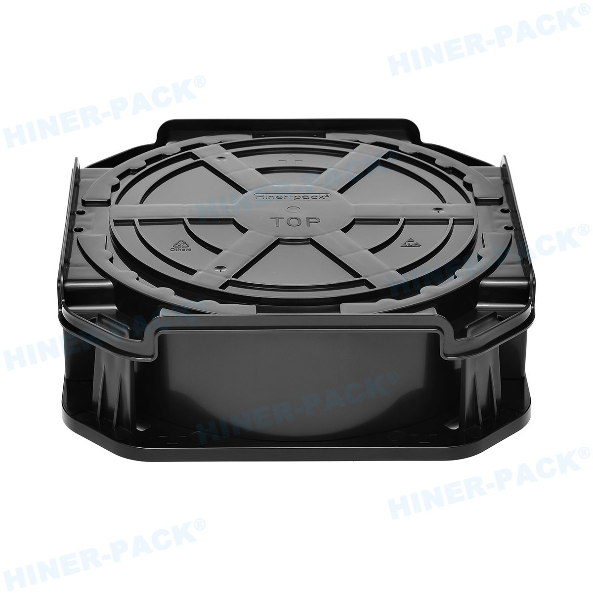
1. Defining Wafer Jars: From Gel Boxes to Vacuum Release Containers
The term wafer jars encompasses several container families
used after wafer dicing or thinning. Three dominant configurations exist in
high-volume manufacturing (HVM):
Gel boxes (tacky gel jars): A rigid plastic jar with a
bottom layer of pressure-sensitive silicone gel that holds a single die or thin
wafer by adhesion. Used for fragile MEMS, compound semiconductors, or ultra-thin
wafers (≤ 100 µm).
Vacuum release jars: A two-part container with a sealing
lid and a valve that allows vacuum packaging. When the vacuum is broken, the lid
releases without particle generation. Preferred for wafer shipping across
fabs.
Static shielding jars: Conductive or dissipative polymer
jars with foam inserts that mechanically trap a wafer without adhesive. Applied
for standard-thickness die (≥ 200 µm) in assembly houses.
Each type requires specific surface resistivity, outgassing profile, and
mechanical shock resistance. Selecting the wrong wafer jar directly correlates with edge chipping, backside contamination, or die shift
during transport.
2. Material Selection for High-Purity and ESD-Safe Wafer Jars
Polymer compounds for wafer jars must satisfy three
conflicting requirements: low outgassing, permanent static dissipation, and
mechanical toughness. Industry data narrows down to three base resins with
tailored additives.
2.1 Polycarbonate (PC) with Carbon Fiber or Conductive Coating
Surface resistivity: 10⁴ – 10⁶ Ω/sq (carbon-filled) or 10⁶
– 10⁹ Ω/sq (coated). Prevents electrostatic discharge (ESD) damage to CMOS or
GaAs devices.
Outgassing (ASTM E595): Total mass loss (TML) 0.35–0.50%;
collected volatile condensable materials (CVCM) < 0.01%. Acceptable for class
100 cleanrooms but not for ultra-high vacuum.
Operating temperature: −40°C to +125°C, sufficient for
warehouse and air transport.
2.2 Polyetheretherketone (PEEK) for High-Temperature or Aggressive Chemical
Exposure
Used when wafer jars must undergo autoclave sterilization or resist solvents
(e.g., NMP, acetone). TML < 0.10%, CVCM = 0.00%.
Surface resistivity achieved via carbon nanotube (CNT) doping: 10³ – 10⁵
Ω/sq.
Cost is 5–8× higher than PC; thus reserved for R&D or medical device
assembly.
2.3 Polypropylene (PP) with Permanent Antistatic Agent
Lower cost alternative for non-critical wafer handling. Resistivity 10⁹ –
10¹¹ Ω/sq.
Potential risk of blooming (antistatic agent migration) over time, causing
surface haze and particle adhesion.
Hiner-pack manufactures wafer jars from medical-grade
PC and PEEK, with lot‑to‑lot verification of resistivity and outgassing using
FTIR and surface resistance meters.
3. Sealing Mechanisms and Environmental Isolation Performance
One primary function of a wafer jar is to create a moisture
and particle barrier. Three sealing technologies dominate, each with
quantifiable ingress protection (IP) ratings.
3.1 Compression Seal with O-Ring (Vacuum Release Jars)
Fluorosilicone or conductive silicone O-ring compressed between lid and
base. Achieves IP67 (immersion up to 1 m for 30 min) and internal relative
humidity < 5% when vacuum-packed with desiccant.
Leak rate testing: Helium leak detector shows < 1×10⁻⁶ mbar·L/s after 100
cycles.
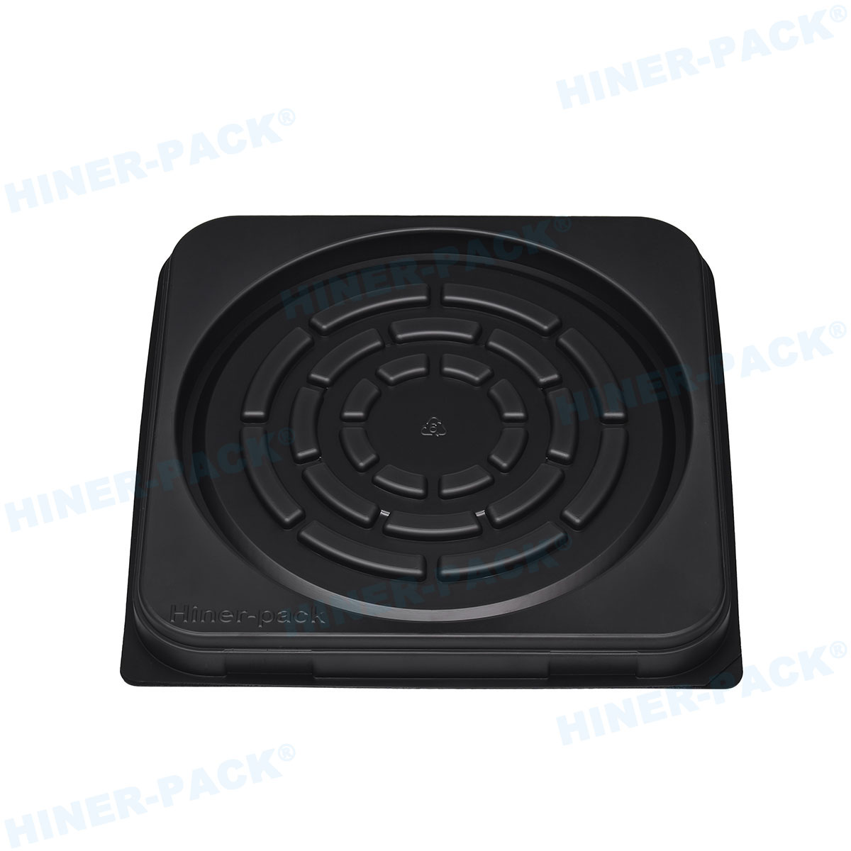
3.2 Labyrinth Seal with Snap Lid (Gel Boxes)
No elastomer; relies on multiple tortuous paths. Prevents particle ingress
down to 1 µm but not moisture tight. Typical moisture ingress rate: 0.5–1.0% RH
per hour.
Suitable for dry nitrogen cabinets or short-term storage (< 48
hours).
3.3 Heat-Sealed Film Overwrap (for Shipping Jars)
4. Particle and Ionic Contamination Control for Wafer Jars
Semiconductor backend fabs require that wafer jars contribute zero yield loss. Industry standard SEMI E46-0321 specifies maximum
particle contribution and ionic residues. Below are actual test methods and
acceptance criteria used by tier-1 OSATs (outsourced semiconductor assembly and
test).
4.1 Liquid Particle Count (LPC) Test
Procedure: Fill the jar with ultrapure water (UPW), agitate ultrasonically
for 5 min, then measure particles ≥ 0.1 µm and ≥ 0.2 µm using a liquid particle
counter.
Acceptance: ≤ 10 particles/ml (≥ 0.1 µm) and ≤ 2 particles/ml (≥ 0.2
µm).
4.2 Ionic Cleanliness by Ion Chromatography
Extract with UPW at 70°C for 1 hour, then analyze for anions (F⁻, Cl⁻, NO₃⁻,
PO₄³⁻, SO₄²⁻) and cations (Na⁺, NH₄⁺, K⁺, Mg²⁺, Ca²⁺).
Limits: Each ionic species < 0.1 µg/cm²; total ionic residues < 0.5
µg/cm².
Failure leads to metal corrosion or die surface leakage current.
4.3 Particle Adhesion Force (for Gel Boxes)
Gel tack force measured by probe tack tester: 100–500 gf (gram-force) for 5
mm probe. Too high tack force makes die removal difficult and leaves gel
residue; too low fails to secure die during vibration.
Residue test: After removing a dummy die, inspect the gel surface under 50×
microscope – no visible transfer.
Wafer jars from Hiner-pack include a
certificate of analysis (CoA) showing LPC and ionic cleanliness per each batch,
enabling audit traceability.
5. Mechanical Shock and Vibration Protection: Data from ISTA Standards
During inter-fab shipping, wafer jars experience random
vibration (1–200 Hz, 0.54 g²/Hz PSD) and mechanical shocks (half-sine 30 g, 6
ms). A properly designed jar must keep the die immobile and edge-protected.
Die retention force: For gel boxes, the gel must withstand
5 g lateral acceleration without die shift. Tested on a vibration table per ISTA
2A.
Compression foam inserts: Closed-cell ESD polyurethane foam
with 10–15% compression set. Density 60–80 kg/m³ ensures that a 300 µm die
experiences contact pressure < 2 psi to avoid fracture.
Drop test performance: A wafer jar containing a silicon die
(200 mm, 150 µm thickness) dropped from 1.2 m onto concrete – edge chipping
probability < 0.5% after 20 drops (ASTM D5276).
Leading suppliers like Hiner-pack perform
simulated shipping tests with accelerometers inside the jar to verify that peak
acceleration transmitted to the die stays below 50 g.
6. Automation Compatibility: Robotic Handling and Machine Vision
Readiness
Modern backend fabs use automated gel box openers, vacuum release jar
unsealers, and conveyor systems. Therefore wafer jars must
include features for reliable machine interaction.
Fiducial marks: Laser-ablated 2D Data Matrix on the jar
base, readable under IR or white light, encoding lot ID and process step.
Kinematic coupling features: Three v-grooves or precision
pads for repeatable positioning (±0.1 mm) on a robotic end-effector.
RFID transponder pocket: Recessed cavity for
high-temperature (150°C) RFID tags, allowing real-time tracking in smart
manufacturing execution systems (MES).
Anti-rotation geometry: Asymmetrical flange or keyway
prevents incorrect loading into a gel box opener.
Hiner-pack offers design customization for all these automation interfaces,
leveraging their in-house polymer R&D base.
7. Quality Management and Certifications for Wafer Jars
End users must demand documented quality evidence. A trustworthy
wafer jar supplier provides:
ISO 9001:2015 and IATF 16949 (automotive-grade) certification for process
control.
Batch records including material certificate, ESD measurement (ANSI/ESD
S541), and outgassing report (NASA/ASTM E595).
Cleanroom manufacturing (Class 7 or better) with final washing in Class 5
laminar flow stations.
Individual bagging: Double-layer ESD shielding bags with humidity indicator
card.
Hiner-pack operates a Class 6 cleanroom for wafer jar
assembly and uses 100% automated optical inspection (AOI) for dimensional
defects and surface contamination.
Integrating Wafer Jars into a Zero-Defect Backend Strategy
Selecting and validating wafer jars is not a commodity decision. From gel tack
force to ionic cleanliness and vibration damping, each parameter affects final
test yield. By working with a vertically integrated manufacturer like Hiner-pack — which combines material science R&D,
injection molding, and certified cleanroom assembly — semiconductor backend fabs
can achieve consistent protection for singulated die and thin wafers. The
industry moves toward fully traceable, ESD-safe, and low-outgassing wafer jars
that support Industry 4.0 automation. Technical due diligence today prevents
field failures tomorrow.
Frequently Asked Questions (FAQ) on Wafer Jars
Q1: What is the difference between a wafer jar and a JEDEC tray or
waffle pack?
A1: A wafer jar typically refers to an
enclosed container (often with a lid and sealing mechanism) that holds a single
wafer or a small number of die. JEDEC trays and waffle packs are open carriers
designed for multiple die in matrix format, used mainly for surface-mount
assembly (pick-and-place machines). Wafer jars provide superior environmental
isolation (moisture/particle barrier) for fragile or sensitive devices during
long-term storage or shipping.
Q2: How do I clean and reuse wafer jars without introducing
contamination?
A2: Reusing wafer jars is not recommended for
critical layers (e.g., 5nm die). If necessary, follow a validated cleaning
protocol: ultrasonic wash with semiconductor-grade surfactant → DI water cascade
rinse → hot air drying (HEPA-filtered) → vacuum bake at 120°C for 2 hours to
remove moisture. After cleaning, requalify LPC and ionic cleanliness. Most fabs
use single-shipment jars to avoid risk. Hiner-pack offers
affordable single-use vacuum release jars for high-reliability shipments.
Q3: Can wafer jars be used for wafers with bumps or micro-structures
(e.g., copper pillars)?
A3: Yes, but the interior surface must be
modified. Standard gel boxes can damage bumps due to gel adhesion forces. Use a
wafer jar with a custom foam insert (soft polyurethane) that
contacts only the wafer edge, or a vacuum release jar with a specialized holder
that supports the wafer by its periphery. Always perform a contact pressure test
(using pressure-sensitive film) before production use.
Q4: What humidity level should be maintained inside a wafer jar for
moisture-sensitive devices (MSL level 2 or 3)?
A4: For MSL2 (≤ 30%
RH exposure allowed before reflow) and MSL3 (≤ 60% RH), the internal humidity of
a sealed wafer jar should be < 5% RH. Achieve this by vacuum-packing the jar
with a desiccant (silica gel or molecular sieve) and including a humidity
indicator card. Vacuum release jars with O-ring seals maintain < 5% RH for
over 6 months when properly sealed.
Q5: How do I validate that a new wafer jar supplier meets SEMI E46
particle requirements?
A5: Request a “cleanliness qualification
report” that includes liquid particle count (LPC) and ionic chromatography
results from an independent lab (e.g., SGS or Eurofins). Perform an in-house
test: place 10 clean dummy wafers in the jars, ship them through your actual
logistics route, then measure particles ≥ 0.1 µm on the wafer surface using a
laser surface scanner. Acceptance: ≤ 0.05 particles/cm² (≥ 0.1 µm) added after
transit.
© 2026 Technical resource for semiconductor packaging and assembly
engineers. For certified wafer jars, gel boxes, and vacuum release containers,
visit Hiner-pack.


