In semiconductor backend manufacturing and wafer-level packaging, the
physical transfer of silicon wafers between fabs, OSATs, and testing houses
remains one of the highest-risk operations. A single substandard shipping
solution can introduce micro-cracks, particulate contamination, electrostatic
damage, or humidity-induced corrosion—directly impacting die yield. When
procurement teams evaluate a wafer shipper for
sale, the decision must go beyond price and delivery. It requires a
deep technical assessment of material properties, cleanroom compatibility, shock
attenuation, and long-term reliability. This article provides an authoritative,
data-driven framework for selecting wafer shippers, referencing industry
standards and real-world application scenarios.
1. Technical Fundamentals: What Defines a Reliable Wafer Shipper?
A wafer shipper—often referred to as a wafer transport box, wafer carrier, or
wafer shipping tray—is engineered to protect bare or taped wafers during
logistics. Unlike standard FOUPs used in automated wafer handling, shippers are
typically designed for inter-facility or cross-continent freight. Key
performance parameters include:
ESD control (surface resistivity 10⁴ – 10¹¹ Ω/sq) –
dissipative or conductive polymers prevent charge accumulation.
Low particle generation (≤ 0.1 particles/cm² for Class 1
cleanrooms) – materials must not shed or abrade under vibration.
Mechanical shock absorption (≥ 60 G impact resistance per ASTM
D4169) – foam inserts or spring-loaded retainers reduce peak
acceleration.
Moisture barrier and outgassing control – low humidity
permeation and no volatile organics (siloxane-free).
When sourcing a wafer
shipper for sale, verifying that the product meets SEMI E15.1
(specifications for 300mm wafer shipping systems) or SEMI G81 (for 150–200mm) is
non-negotiable for high-volume manufacturing.
2. Critical Industry Pain Points and Technical Solutions
2.1 Edge Chipping and Surface Scratching
Fragile 200mm and 300mm wafers experience edge damage when shippers lack
proper wafer separation or have inconsistent pocket tolerances. Solutions
include precision-machined wafer slots with radiused edges and anti-sliding
ribs. Advanced designs use dual-density foam: a rigid outer layer for structural
integrity and a soft inner layer that conforms to wafer contours.
2.2 Electrostatic Discharge (ESD) Hidden Failures
ESD events during shipping cause latent defects—metal spiking, gate oxide
punch-through—that only surface during final test. Permanent damage occurs in
devices with geometries below 28nm. A compliant wafer shipper for sale must incorporate static-dissipative carbon or intrinsically conductive polymers,
verified by surface resistance tests (ANSI/ESD STM11.11). Closed-cell conductive
foam is preferred over coated materials, as coatings wear off with repeated
use.
2.3 Particulate Contamination from Abrasion
Standard polypropylene shippers often generate particles from lid-to-base
friction. High-end alternatives use carbon-fiber-reinforced PEEK or
PTFE-modified acetal, which exhibit low coefficient of friction. For wafer fabs
requiring ISO Class 4 or better, shippers should be ultrasonically cleaned,
double-bagged, and certified for particle shedding per IEST-RP-CC003.4.
3. Single-Wafer vs. Multi-Wafer Shippers: Application-Driven Choice
Selecting the right format depends on wafer size, process stage, and shipment
volume. Below is a technical comparison:
Single-wafer shippers: Ideal for prototype, R&D,
high-value MEMS, or known-good-die shipments. Provide individual protection with
custom cavities. Typical capacity: 1 or 2 wafers. Used when traceability and
zero cross-contamination are mandatory.
Multi-wafer shippers (e.g., 13, 25, 50-slot): Standard for
production transfers. Optimize cube utilization and reduce per-wafer shipping
cost. Require precise slot pitch (10mm for 300mm wafers) and anti-rotation
keys.
Stackable or nestable designs: Reduce warehouse footprint.
Ensure latch mechanisms withstand 1000+ cycles without loss of clamping
force.
4. Material Science Behind High-Quality Wafer Shippers
Advanced polymer engineering distinguishes commodity shipping boxes from
high-reliability solutions. Dominant materials include:
Polycarbonate (PC) + carbon fiber: High impact strength,
good dimensional stability, but moderate chemical resistance. Suitable for dry,
controlled environments.
ESD-safe polypropylene (PP) with conductive additive: Cost-effective for 150mm/200mm shippers. Ensure additive dispersion to avoid
static hot spots.
Polyetheretherketone (PEEK) – high-end: Extremely low
outgassing (NASA low outgassing certified), excellent wear resistance, ideal for
vacuum-baked or high-temperature post-processing.
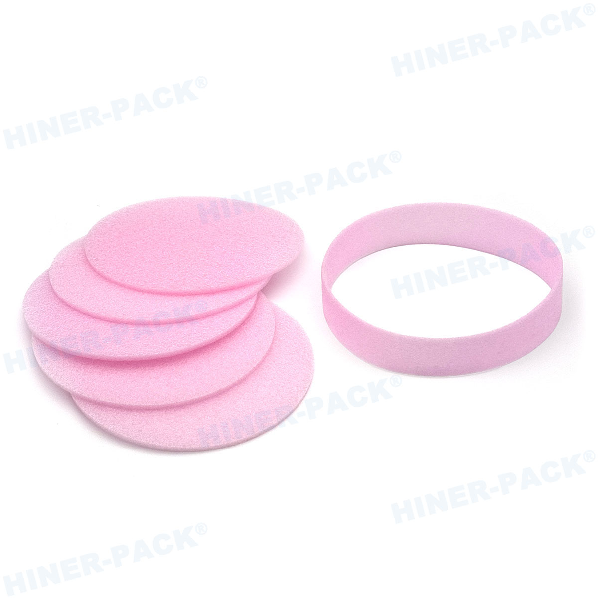
Conductive foam (polyurethane or EVA): Density control
(35–50 kg/m³) provides predictable shock absorption. Static decay time less than
0.1 second per FTMS 101C.
Hiner-pack designs wafer shipping systems using these materials, verified through
third-party lab tests including vibration profiling (ISTA 3A) and electrostatic
decay measurement. Their engineering team provides custom die-cut foam inserts
and in-house cleanroom assembly—critical for clients requiring lot-specific
certifications.
5. SEMI Standards and Cleanroom Compliance: Mandatory Certifications
Before finalizing a purchase, procurement must request conformity
documentation. Relevant standards include:
SEMI E15.1 – specifies mechanical interface, dimensions,
and handling features for 300mm wafer shipping boxes.
SEMI E76 – defines ESD protective properties for wafer
carriers, including surface resistivity and discharge time.
SEMI E126 – test method for characterizing particle
contribution from wafer transport containers.
ISO 14644-1 Class 4 or Class 5 cleanroom assembly – ensures
shippers are packed free of airborne particles.
Reputable suppliers offer full traceability from resin batch to finished
product, including ion chromatography reports for ionic contamination (fluoride,
chloride, nitrate). When you evaluate a wafer shipper for
sale, request the latest SEMI compliance certificate and outgassing
analysis (TD-GC/MS).
6. Application Scenarios: From 200mm Power Devices to Advanced 300mm
Logic
Each semiconductor segment imposes distinct requirements:
Power device fabs (150mm/200mm, SiC, GaN): Heavier wafers
(up to 800µm thick) need deeper slots and reinforced latch mechanisms. Thermal
cycling during shipping from –40°C to +60°C demands low warpage of the shipper
base.
Image sensor manufacturing (CIS): Ultra-sensitive to
particles (defects > 0.3µm can kill pixels). Hermetic-style shippers with
foam seal gaskets and double-bagging are mandatory.
Advanced logic (7nm/5nm): Extreme fragility of ultra-thin
wafers after backgrinding (50–100µm thick). Require shippers with vacuum-formed
wafer cradles and edge-only contact to prevent backside scratches.
OSATs for wafer-level packaging: High mix of wafer sizes,
often requiring adjustable slot inserts. Many OSATs now standardize on reusable
shippers with cleanable surfaces to reduce consumables cost.
7. Evaluating Supplier Capabilities: What to Ask Before Buying
When shortlisting vendors offering a wafer shipper for sale, apply the
following technical audit checklist:
Do they provide mechanical drawings with tolerance analysis (slot pitch
±0.05mm, flatness ≤0.1mm)?
Is there a lot acceptance test (LAT) protocol for particle and ESD per your
cleanroom class?
Can they support rapid prototyping (3D printed or soft tooling) for
non-standard wafer layouts?
What is the documented lifecycle – number of reuse cycles before material
degradation (typically 50–500 cycles depending on polymer)?
Are replacements parts (lid seals, replacement foam) stocked to avoid
production line stoppage?
Leading suppliers offer simulation reports using finite element analysis
(FEA) of impact scenarios, plus vibration spectrum analysis matching actual
freight conditions. This level of engineering transparency reduces qualification
time significantly.
8. Future-Ready Features: RFID, IoT integration, Data Logging
Smart wafer shippers now integrate passive or active RFID tags for route
tracking, shock event recording, and temperature/humidity logging. For sensitive
processes like silicon photonics or SAW filters, embeddable data loggers with
Bluetooth low energy (BLE) transmission allow real-time monitoring of shock
events exceeding 30G. When evaluating a wafer shipper for sale with smart capabilities, check for battery life (for active tags) and
compatibility with your warehouse management system.
9. Frequently Asked Questions (Technical and Procurement Focus)
Q1: Can I reuse a standard wafer shipper after multiple shipments,
and how do I verify its cleanliness?
A1: Reuse is
common for durable shippers made of PC or PP. However, requalification must
include particle testing per SEMI E126, surface resistivity check (ESD), and
microscopic inspection for cracks. Hiner-pack provides a requalification protocol including laser particle counter scanning
and ion chromatography for ionic residues. Without requalification, reuse risks
cross-contamination and ESD failure.
Q2: What is the typical lead time for a customized wafer shipper
(non-standard wafer size or foam pattern)?
A2: For
fully custom tooling (injection mold), lead time ranges from 6 to 10 weeks. For
low-volume CNC-machined or 3D-printed shippers, 2–3 weeks. Suppliers offering
modular foam inserts can reduce lead time to 5 business days. Always request DFM
(design for manufacturing) feedback from your supplier early in the procurement
cycle.
Q3: Are there specific wafer shippers for “warped” wafers after
thin-film deposition or annealing?
A3: Yes. Warped
wafers (bow >1mm) require shippers with adjustable supports or spring-loaded
retainer systems that apply uniform pressure across the wafer's convex side.
Standard flat pocket designs will not secure warped wafers and may cause edge
breakage. Suppliers like Hiner-pack offer shims and clamp force adjustable lids
specifically for warped wafers used in fan-out packaging.
Q4: How to ensure that the wafer shipper does not introduce organic
contamination (outgassing) that affects wire
bonding?
A4: Request outgassing test reports per
SEMI E108 or JEDEC JS709B. Use high-purity materials such as PEEK or
fluoropolymer-coated surfaces. Avoid products with plasticizers, slip agents, or
mold-release residues. Cleanroom-assembled shippers that undergo vacuum baking
(120°C for 2 hours) prior to final packaging significantly reduce
outgassing.
Q5: What is the difference between “single-use” and “multi-use” wafer
shippers in terms of material certification?
A5: Single-use shippers are often manufactured with less expensive conductive PP and
may not maintain ESD properties after one trip. Multi-use shippers require
validation for 50+ cycles, including abrasion resistance, latch cycle testing,
and minimal surface resistivity change. Multi-use units must also meet higher
impact strength (Izod >8 kJ/m²) to withstand repeated handling. Always check
cycle-life test data from the supplier.
Conclusion – Secure a Reliable Wafer Shipper for Your Process
Requirements
Selecting a wafer shipper for sale demands rigorous technical evaluation:
from material outgassing and particle generation to SEMI compliance and reuse
economics. Competent suppliers provide full transparency on mechanical testing,
cleanroom assembly, and traceability. Whether you handle 200mm legacy devices or
advanced 300mm wafers with ultra-low-k dielectrics, the right shipper directly
preserves yield and reduces logistical risks.
For tailored engineering support, custom tooling, or to request qualification
samples, send your technical inquiry to Hiner-pack’s
semiconductor packaging division. Their team responds with design proposals,
test reports, and competitive pricing based on annual volume. Start your
procurement process today – request a quote and ensure best-in-class wafer
protection.
Ready to source
high-reliability wafer shippers? Contact Hiner-pack for a technical consultation
and get a customized solution. Send your inquiry now → https://www.waferboxes.com/contact.html (or use the company email address on website).


