
In semiconductor front-end and back-end logistics, the interface between each wafer within a shipper determines the risk of particle generation, static discharge, and edge chipping. The wafer shipper separator is a precision component that must balance cushioning, cleanliness, and dimensional consistency. This article reviews failure modes observed in 300 mm and 200 mm wafer shipping environments, providing quantifiable selection guidelines. Hiner‑pack has supplied cleanroom‑grade separators to leading foundries and OSATs for over 15 years, and their engineering data informs the technical recommendations below.
1. The Functional Role of a Wafer Shipper Separator in Safe Transport
Wafer shippers (plastic or metal carriers) hold multiple wafers in a stacked configuration. Without a wafer shipper separator, adjacent wafers would contact each other, causing friction damage and particle shedding. The separator serves three critical purposes:
Spacing maintenance: Maintains a precise gap (typically 3–6 mm) between wafers to prevent contact during vibration or shock.
Contamination barrier: Prevents transfer of particles or moisture from one wafer surface to another.
ESD path control: Provides a controlled discharge path to avoid electrostatic accumulation on sensitive device wafers.
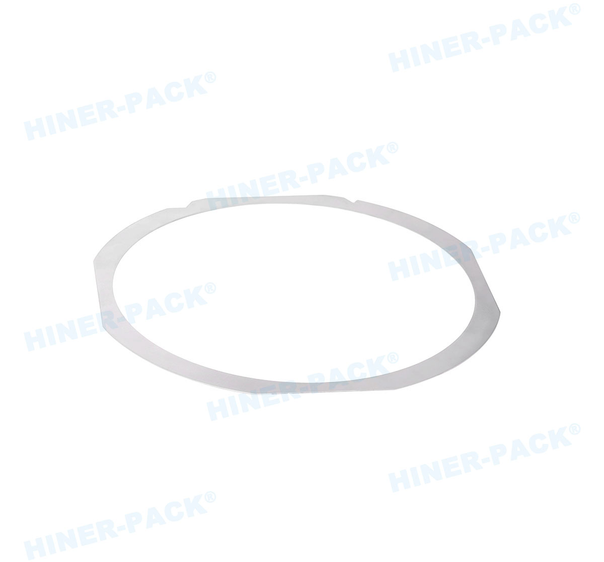
A poorly designed wafer shipper separator can cause edge chipping, surface micro‑scratches, or electrostatic damage (ESD). For 300 mm wafer fabs, the tolerance on separator flatness is as tight as ±0.05 mm to ensure uniform pressure distribution across the wafer backside. Hiner‑pack manufactures separators with a polished contact surface (Ra ≤ 0.2 µm) to eliminate abrasive points.
2. Material Selection: Cleanroom‑Compatible Polymers and Fillers
The base material of a wafer shipper separator must resist outgassing, chemical attack, and dimensional change under temperature fluctuations. Four material families dominate the wafer transport accessories market:
Polypropylene (PP) – conductive grade: Surface resistivity 10³–10⁵ Ω/sq. Low cost, good chemical resistance to isopropyl alcohol (IPA) and dilute acids. Suitable for 200 mm shippers in non‑critical environments. However, PP has limited stiffness (flexural modulus ≈1.5 GPa) and may warp under heavy stacking.
Polycarbonate (PC) – antistatic: Higher stiffness (2.4 GPa) and clarity. Used for visual inspection of wafers without removing separators. Antistatic version (10⁹–10¹¹ Ω/sq) is common. PC is susceptible to stress cracking in contact with acetone or strong bases.
PEEK (polyether ether ketone) – electrostatic dissipative (ESD): Surface resistivity 10⁶–10⁹ Ω/sq. Withstands 260°C, compatible with aggressive solvents (NMP, THF). Used in high‑temperature baking processes. PEEK separators are mandatory for GaAs or SiC devices where ionic contamination is strictly controlled.
PPS (polyphenylene sulfide): Excellent creep resistance and low moisture absorption (0.02%). Often specified for automated wafer handling where separators are picked and placed by vacuum grippers.
For a typical 300 mm foundry shipping bare silicon wafers, an antistatic polycarbonate wafer shipper separator offers the best balance of cost and performance. However, if the wafer shipper undergoes a 150°C bake cycle (e.g., for moisture removal), PEEK or PPS is required. Hiner‑pack’s PEEK separators are injection‑molded with a special gate design that minimizes weld lines and ensures uniform flatness.
3. Dimensional Specifications: Thickness, Flatness, and Concentricity
Every wafer shipper separator must be measured against three critical dimensions:
Thickness uniformity: For 300 mm separators, nominal thickness is 1.0–1.5 mm. Variation across the diameter must be ≤ ±0.03 mm. Thicker separators reduce shipper capacity; thinner ones risk warping.
Flatness (total indicator runout): Measured on a granite plate, flatness should be ≤0.05 mm for 200 mm separators and ≤0.03 mm for 300 mm. Non‑flat separators cause uneven pressure and wafer bow.
Outer diameter (OD) and inner diameter (ID): The OD must match the shipper’s inner groove (typically 310–315 mm for 300 mm shippers). The ID (clearance hole for wafer center) is usually 100–120 mm. Any eccentricity >0.2 mm can cause the separator to shift during transport, leading to wafer edge contact.
A common failure mode is “separator creep” – after repeated use, the separator’s OD shrinks due to compression set. This is measured by comparing the separator’s OD after 100 shipping cycles. High‑quality PEEK separators from Hiner‑pack maintain OD within ±0.1 mm for over 500 cycles. Low‑grade PP separators can shrink by 0.5 mm after only 50 cycles, causing the stack to collapse.
4. Cleanliness Levels: Particle Shedding and Ionic Contamination
Semiconductor wafers are extremely sensitive to particles ≥0.1 µm. The wafer shipper separator must be manufactured and packaged under cleanroom conditions (Class 100 / ISO 5) and tested for:
Particle generation: Using liquid particle counting (LPC) or surface particle extraction. Specification: ≤10 particles/cm² of size ≥0.3 µm; ≤1 particle/cm² of size ≥1.0 µm.
Outgassing (dynamic headspace analysis): Total volatile organic compounds (TVOC) < 10 µg/g, with no siloxanes or plasticizers that could deposit on wafer surfaces.
Ionic extractables (ICP‑MS): Sodium, potassium, chloride, and fluoride ions each < 0.1 µg per separator.
Many low‑cost wafer shipper separators fail these tests because they are molded from recycled resins or use mold release agents. Hiner‑pack operates a dedicated cleanroom molding line, with each batch of separators certified to meet or exceed SEMI E78 (particle) and SEMI E49 (outgassing) standards. The company provides a certificate of analysis (COA) for every shipment.
5. Industry Pain Points: Wafer Edge Chipping, Cross‑Contamination, and Static Damage
Based on field failure analysis from six 300 mm fabs, three recurring problems are directly linked to poor wafer shipper separator design or wear:
Edge chipping: Caused by separators with sharp inner or outer edges. Mitigation: specify a chamfered or radiused edge (R0.3–0.5 mm) on both sides. Inspect new separators with a 50× microscope for burrs.
Cross‑contamination from previous lots: Porous or scratched separators trap residues. Use non‑porous, smooth surface materials (PEEK or polished PC). Implement a separator cleaning protocol: ultrasonic bath with deionized water and 2% semiconductor‑grade detergent, followed by rinse and nitrogen dry.
ESD damage to sensitive devices: Insulating separators (surface resistivity >10¹² Ω/sq) allow charge buildup. When a wafer is lifted, a static discharge can occur through the device circuitry. Always specify ESD‑safe separators with surface resistivity between 10⁶ and 10⁹ Ω/sq, measured according to ANSI/ESD STM11.11.
An often overlooked solution is separator edge polishing. Hiner‑pack’s wafer shipper separator undergoes a secondary tumble‑polishing step that removes micro‑burrs, reducing edge chipping incidents by 70% in customer audits.
6. Compatibility with Automated Shipping and Handling Equipment
Modern wafer fabs use automated material handling systems (AMHS) that open shippers and extract wafers using vacuum end effectors. The wafer separator must be compatible with:
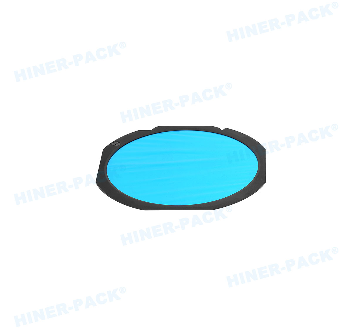
Vacuum pick‑up points: Many separators feature three or four dimples or raised bosses that match the end effector’s suction cups. Without these, the separator cannot be reliably removed.
Orientation features: Notches or flats on the separator’s OD that align with the shipper’s key to prevent incorrect insertion.
Stack height sensors: The separator’s thickness must be consistent enough that the shipper’s optical sensor can count the number of wafers and separators correctly. A ±0.05 mm thickness variation can cause miscounts.
When sourcing a wafer shipper separator, provide the AMHS brand (e.g., Muratec, Daifuku, Brooks) and the end effector model. Hiner‑pack maintains a library of over 100 custom separator geometries, including those for FOUP (front opening unified pod) and H‑Square shippers. Their engineering team can reverse‑engineer an existing separator within 5 days.
7. Cleaning and Reuse Protocols: Maximizing Separator Lifetime
While some fabs treat separators as single‑use, cost pressures drive reuse. A well‑designed wafer shipper separator can withstand 100–300 cleaning cycles if proper procedures are followed:
Cleaning chemistry: Use semiconductor‑grade surfactants (e.g., 2% Versaclean) in deionized water at 40–50°C. Avoid strong bases (pH >11) on PC, and avoid acetone on any polymer.
Ultrasonic parameters: Frequency 40 kHz, power density 10–20 W/L, duration 5–10 minutes. Excessive ultrasonic energy can erode the separator surface and increase particle shedding.
Drying: Forced nitrogen at 60°C for 30 minutes, or vacuum drying at 50°C. Air drying leaves water spots that can later release ions.
Inspection after cleaning: Visual check under 10× magnification for cracks, warpage, or discoloration. Reject any separator with visible damage.
Hiner‑pack offers a separator recertification service: customers send used separators to their cleanroom, where they are ultrasonically cleaned, inspected, and repackaged with a new COA. This extends separator life by up to 500 cycles, reducing consumables cost by 40%.
Frequently Asked Questions (FAQs) About Wafer Shipper Separators
Q1: Can I use the same wafer shipper separator for different wafer
sizes (e.g., 200 mm and 150 mm)?
A1: No. The
separator’s outer diameter is matched to the shipper’s inner diameter, which is
specific to the wafer size. A 200 mm wafer shipper has a different groove
diameter than a 150 mm shipper. Using a mismatched separator can cause the wafer
to slide or the separator to tilt, leading to edge damage. Always order
separators that exactly match your shipper model and wafer diameter.
Q2: How do I measure the surface resistivity of a wafer shipper
separator on site?
A2: Use a concentric ring probe
(e.g., ACL 800) connected to a megohmmeter compliant with ANSI/ESD STM11.11.
Place the probe on a clean, dry area of the separator, apply 10–100 V, and
record the reading after 15 seconds. For accurate results, measure at three
different locations. Acceptable range: 10⁶ to 10⁹ Ω/sq for ESD‑safe separators.
Hiner‑pack provides a resistivity measurement report with every shipment.
Q3: What is the typical particle generation limit for a new wafer
shipper separator?
A3: According to SEMI E78-0718,
a Class 1 separator must generate ≤5 particles ≥0.3 µm per cm² and ≤0.1
particles ≥1.0 µm per cm² when tested using liquid particle counting (LPC).
Hiner‑pack’s wafer shipper
separators typically achieve ≤2 particles/cm² (≥0.3 µm) and ≤0.05
particles/cm² (≥1.0 µm), meeting the strictest foundry requirements.
Q4: Can wafer shipper separators be autoclaved or steam
sterilized?
A4: Only PEEK and certain PPS grades
can withstand autoclave conditions (121°C, 15 psi, saturated steam).
Polycarbonate and polypropylene will warp or hydrolyze. If your process requires
sterilization (e.g., for medical device MEMS), specify PEEK separators.
Hiner‑pack offers autoclave‑compatible PEEK separators with validated
dimensional stability after 50 cycles.
Q5: How do I prevent separator sticking to wafers after long‑term
storage?
A5: Sticking occurs due to electrostatic
attraction or moisture film formation. Solutions: (1) Use antistatic separators
(surface resistivity 10⁶–10⁹ Ω/sq) to dissipate charge. (2) Store shippers in a
dry nitrogen purge cabinet (relative humidity <20%) to eliminate moisture
bridging. (3) If sticking persists, apply a thin layer of semiconductor‑grade
ionizer air before opening the shipper. Avoid any lubricants or release agents
on the separator surface.
Q6: Are there color‑coded wafer shipper separators for lot
identification?
A6: Yes. Many fabs use blue, green,
or yellow separators to visually distinguish different process flows or device
types. The color is achieved by adding a cleanroom‑compatible masterbatch that
does not affect electrical or outgassing properties. Hiner‑pack offers color
coding on request, with a minimum order of 200 pieces per color. The pigment
system is certified to contain no heavy metals or halogens.
Prioritize Cleanliness and Dimensional Traceability
The wafer shipper separator is a low‑cost consumable, but its impact on wafer quality is substantial. A separator with verified flatness, controlled particle emission, and proper ESD properties prevents edge chipping, cross‑contamination, and static failures. For high‑volume fabs and OSAT facilities, establishing a supplier qualification program that includes material certificates, particle testing, and dimensional reports is a best practice.
Ready to specify wafer shipper separators for your 200 mm or 300 mm line? Provide your shipper brand and model, wafer size, required cleanliness class, and monthly volume. Hiner‑pack’s engineering team will recommend the optimal material, provide samples for validation, and include a full certificate of analysis with every shipment.
Request a quote or technical datasheet: Send your separator
specifications →
For urgent inquiries, email
rainbowzhu@hiner-pack.com with subject “Separator inquiry – [wafer
size]” for a 4‑hour response.


