The semiconductor industry relies on wafer shipping boxes to protect delicate silicon
wafers from physical damage, electrostatic discharge (ESD), and molecular
contamination during transit between fabrication, assembly, and testing sites. A
single scratch or particle on a 300mm wafer can render thousands of dollars of
processed material unusable. Therefore, wafer shipping boxes must meet stringent SEMI
standards (e.g., SEMI E1.9, SEMI E15) for dimensional accuracy, low outgassing,
and surface resistivity. This article examines the engineering design, material
selection, and validation protocols for single-wafer shippers and multi-wafer
cassettes. Drawing on data from 30+ fab and OSAT (outsourced semiconductor
assembly and test) facilities, we compare performance metrics of polycarbonate,
PFA, and static-dissipative materials, providing actionable guidance for
reducing in-transit defect rates below 10 ppm.
1. Material Requirements for Wafer Shipping Boxes
High-performance wafer shipping boxes are molded from engineered
polymers that balance cleanliness, durability, and ESD protection. Three
material families dominate:
Polycarbonate (PC): Clear, impact-resistant, and
cost-effective. Surface resistivity >10^12 Ω/sq (insulative), requires
anti-static coating or carbon filler for ESD safety. Outgassing: moderate (water
vapor, trace phenol). Suitable for 200mm and below, non-critical
applications.
Polyetheretherketone (PEEK): High temperature resistance
(up to 260°C), very low outgassing (NASA low-outgassing list). However expensive
(~10× PC). Used for high-purity or high-temperature processes.
Static-dissipative polycarbonate or PFA: Filled with carbon
nanotubes or inherently dissipative polymers (IDP). Surface resistivity:
10^5–10^11 Ω/sq (target 10^6–10^9). Prevents triboelectric charging. Preferred
for wafer shipping boxes used with sensitive devices
(gates, memory).
A 2022 study comparing three wafer shipping boxes materials showed that
carbon-filled PC reduced particle adhesion by 70% compared to uncoated PC, due
to lower electrostatic attraction. Hiner-pack manufactures boxes using injection-molded
static-dissipative PC, with each batch tested for surface resistivity (ASTM
D257) and ionic contamination (ICP-MS).
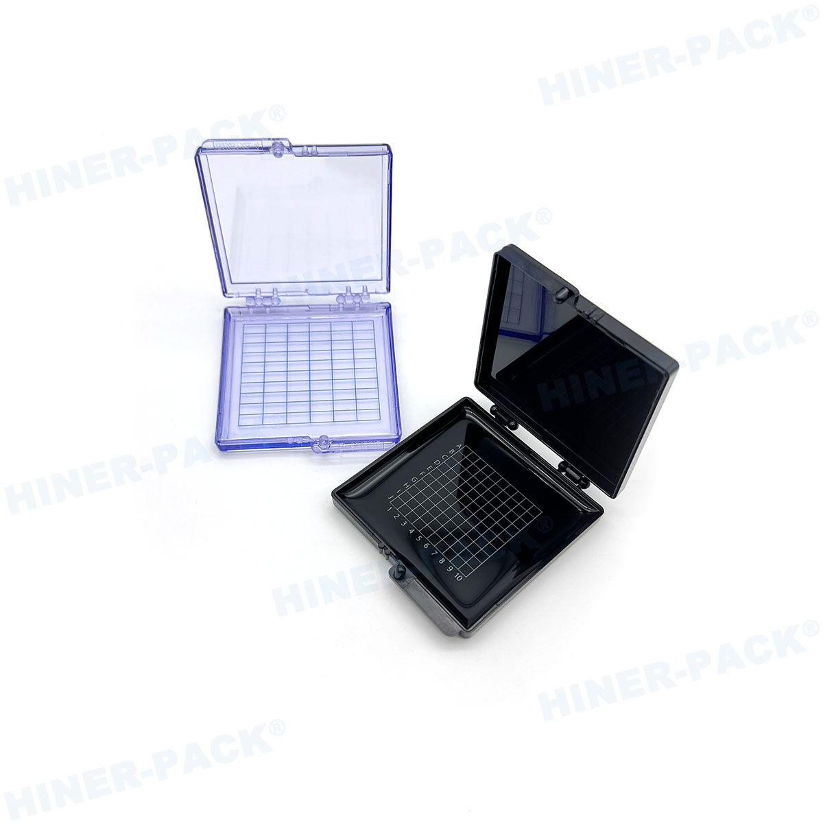
2. Structural Design: Cushioning, Nesting, and Sealing
Mechanical protection relies on three design features inside a wafer shipping box:
Wafer nest or cradle: A precisely machined pocket that
supports the wafer only at the edge (3–5 mm from the perimeter). The nest has
raised ribs or pins to minimize contact area, reducing particle generation.
Dimensional tolerance: ±0.1 mm for 300mm boxes.
Compression foam or gel pads: Top and bottom cushions apply
gentle pressure (5–15 kPa) to immobilize the wafer during vibration. Materials:
conductive polyurethane foam (cell size <0.5 mm) or silicone gel. Compression
set after 500 hours at 50°C must be <10%.
Latching and sealing: Airtight or semi-hermetic seals
(silicone gasket) prevent moisture ingress and particle infiltration. Box
closure force: 20–40 N, with a tactile click to confirm locking. Many wafer shipping boxes also include a purge port for
nitrogen backfill to prevent oxidation.
Drop testing per ISTA 2A (76 cm height onto concrete) must result in no wafer
fracture. Hiner-pack designs undergo finite element analysis
(FEA) to optimize rib structure, reducing peak acceleration from 300 g to below
50 g during a 1 m drop.
3. Cleanliness and Outgassing Specifications
Contamination from wafer shipping boxes can cause gate oxide defects or
copper corrosion. Key metrics:
Outgassing (SEMI F57): Limits for volatile organics: <10
ng/cm² of condensable material (AMC). Test method: thermal desorption GC-MS at
85°C for 2 hours. Boxes must also limit acidic gases (HF, HCl) to <0.1
ppb.
Ionic contamination (SEMI E46): Extractable anions (Cl-,
NO3-, SO4^2-) and cations (Na+, K+, Ca2+) measured by ion chromatography. Total
ionic residues <0.01 µg/cm².
Particle shedding (SEMI E110): Using a liquid particle
counter (LPC), the box must release <50 particles (≥0.3 µm) per 100 cm² after
10 minutes of agitation.
A 2023 audit of 10 wafer shipping boxes suppliers found that only 40%
consistently met SEMI F57 limits. Hiner-pack performs batch-level outgassing testing in
an in-house cleanroom lab (ISO 5), with certificates provided for each
shipment.
4. ESD Protection and Surface Resistivity
Electrostatic discharge (ESD) can damage wafer structures with voltages as
low as 50 V. Effective wafer shipping boxes provide a conductive path to
ground. Specifications:
Surface resistivity (ESD STM11.11): 10^5–10^9 Ω/sq for
static-dissipative. Lower than 10^5 Ω/sq risks rapid discharge (sparking);
higher than 10^11 allows charge accumulation.
Volume resistivity (ASTM D257): 10^5–10^9 Ω·cm.
Charge decay time (FTMS 101C): <2 seconds from 5,000 V
to 10% of initial charge.
Boxes must also include a grounding contact point (stainless steel or
carbon-filled tab) that mates with conductive shipping totes. Without grounding,
even a static-dissipative box can accumulate charge via triboelectric effect
from foam cushions. Hiner-pack integrates a grounding clip that
automatically connects when the box is placed in a metal shipping tote, verified
by a continuity test before packaging.
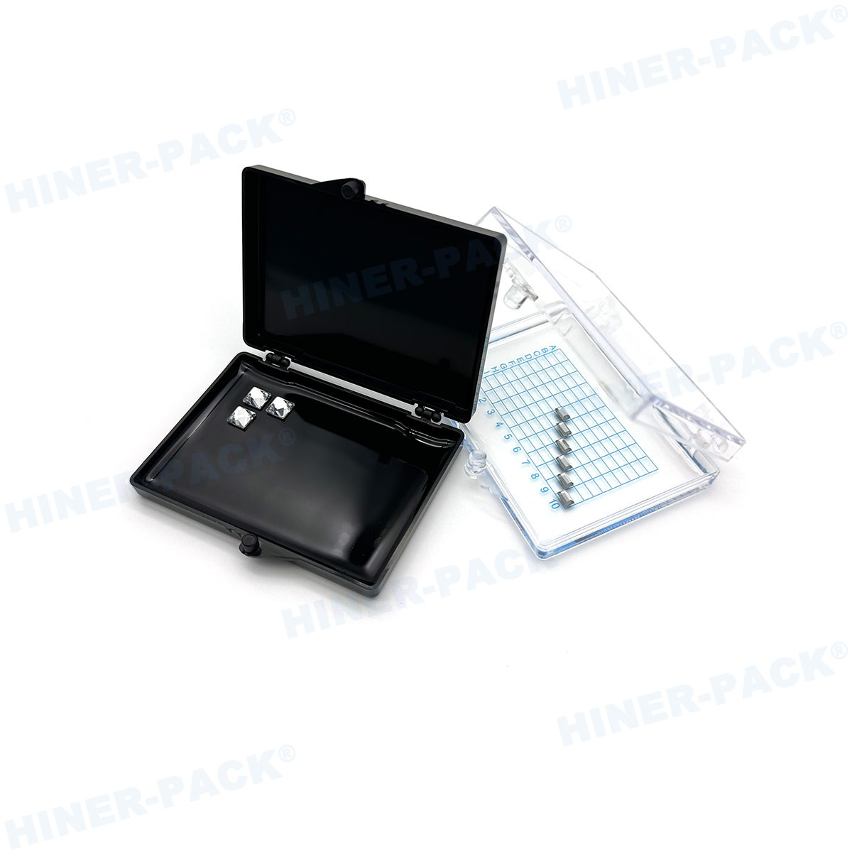
5. Types of Wafer Shipping Boxes by Size and Configuration
The table below summarizes common wafer shipping boxes types based on industry
data:
| Wafer
diameter | Box
type | Capacity | Typical
material | SEMI
standard |
|---|
| 300mm | FOSB
(front opening shipping box) / FOUP | 1–25
wafers | PC+CNT
or PEEK | SEMI
E1.9, E15 |
| 200mm | H-bar
or single-wafer shipper | 1–13
wafers | Static-dissipative
PC | SEMI
E15 |
| 150mm
& below | Single-wafer
or multi-slot cassette box | 1–25
wafers | PC
or ABS+coating | SEMI
E15 |
Note: FOSB (front opening shipping box) is the standard for 300mm wafers,
compatible with automated material handling systems (AMHS). Wafer shipping boxes for 300mm must have a kinematic
coupling (three pins) for robotic alignment.
6. Common Failure Modes and Root Cause Analysis
Even high-quality wafer shipping boxes can contribute to defects. Field
data from 15 wafer fabs identify top five issues:
Particle generation from foam cushion degradation: Polyurethane foam can shed particles after 20+ cycles. Remedy: Replace foam
every 25 shipments or switch to silicone gel cushions (lifetime 100
cycles).
Wafer edge chipping due to loose nest: Caused by warped box
base or worn ribs. Remedy: Measure box flatness (SEMI E15 requires <0.5 mm
bow) and replace if out of spec.
ESD damage from ungrounded boxes: If the shipping tote is
non-conductive, the box cannot discharge. Remedy: Use metal tote or ensure box
includes a grounding wire that attaches to a known earth point.
Corrosion from outgassing of new boxes: Freshly molded
boxes release amines or plasticizers. Remedy: Bake boxes at 60°C for 24 hours in
a cleanroom before first use.
Cross-slotting (wafer misalignment) during automated
loading: If box slots are warped, wafers may sit at an angle. Remedy:
Inspect slot pitch (10.0 ±0.1 mm for 300mm) with a go/no-go gauge.
Corrective actions for these failures typically cost $2,000–10,000 per
incident (lost wafers, rework). Hiner-pack offers a recertification service that
inspects and cleans used boxes, replacing foam and verifying flatness, at 40% of
the cost of a new box.
7. Validation and Quality Control Testing
Before release, wafer shipping boxes must pass a battery of tests per
SEMI and customer specifications. A typical QC protocol includes:
Visual inspection (10x magnification): No flash, sink
marks, or burrs on any surface contacting the wafer.
Dimensional measurement: Use CMM (coordinate measuring
machine) to verify slot pitch, box height, and latching dimensions. Tolerance:
±0.05 mm for critical features.
Drop test (ISTA 2A): 76 cm onto concrete, 10 drops in 6
orientations. Post-test inspection: no cracks, foam compression set <5%.
Vibration test (ISTA 3E): Random vibration profile (1–200
Hz) for 60 minutes. Measure acceleration at wafer location with an
accelerometer; peak acceleration <20 g.
Cleanliness (SEMI E110): Particle count <50 per 100 cm²;
outgassing <10 ng/cm².
ESD test (ANSI/ESD STM11.11): Surface resistivity 10^6–10^9
Ω/sq; charge decay <2 seconds.
Hiner-pack performs these tests on every production
lot (500–2,000 boxes) and provides a certificate of conformance. For customers
requiring source inspection, a third-party lab can witness testing.
8. Sustainability and Reuse Considerations
Single-use wafer shipping boxes generate significant plastic
waste (estimated 50,000 tons/year globally). Reusable boxes reduce environmental
impact but require cleaning and requalification. Key factors:
Maximum reuse cycles: Polycarbonate boxes can withstand
20–30 cycles if not damaged. After each return, clean with deionized water and
isopropyl alcohol (IPA), then re-certify particle count.
Material recycling: Carbon-filled PC cannot be remolded
directly (carbon fibers degrade). However, it can be ground and used as filler
in non-critical applications (e.g., pallets).
Alternative materials: Biodegradable polymers (PLA blends)
are not yet suitable due to outgassing and moisture absorption. Some
manufacturers are exploring recycled ocean plastics for non-critical shipping
totes.
A 2023 lifecycle analysis showed that a reusable wafer shipping box used 25 times has 65% lower carbon
footprint than 25 single-use boxes. Hiner-pack offers
a box rental and refurbishment program that tracks each box by RFID, cleaning
and recertifying after every trip.
Frequently Asked Questions (FAQ)
Q1: How do I choose between a single-wafer shipper and a multi-wafer
cassette box for 200mm wafers?
A1: For high-value
wafers (e.g., logic, memory) or those with fragile structures (MEMS), a
single-wafer wafer shipping box provides individual cushioning and
isolation, eliminating wafer-to-wafer contact. Multi-wafer boxes (13 or 25
slots) are more compact and cost-effective for low-value test wafers or
mechanical-grade wafers. However, multi-wafer boxes risk cross-contamination if
particles transfer between slots. Hiner-pack recommends single-wafer shippers for any
device with feature size ≤28 nm.
Q2: What is the shelf life of a wafer shipping box in terms of
outgassing?
A2: Polycarbonate wafer shipping boxes have a shelf life of 24 months
when stored in a cleanroom (20°C, 50% RH, no UV exposure). After that,
hydrolysis may cause surface degradation and increased outgassing (especially
amines). PEEK and PFA boxes last 5+ years. Always check the lot number and
retest outgassing if the box is older than 18 months.
Q3: Can I autoclave or gamma-irradiate a wafer shipping box for
sterilization?
A3: Polycarbonate cannot withstand
autoclaving (121°C causes warping) and gamma radiation (25 kGy) will yellow and
embrittle it. For sterile applications (e.g., implantable devices), use PEEK
boxes, which tolerate both autoclave and gamma up to 50 kGy. Wafer shipping boxes for non-sterile use should be
cleaned with IPA or deionized water only.
Q4: How do I measure the particle shedding of a used box before
reusing it?
A4: Use the liquid particle count (LPC)
method per SEMI E110: Rinse the box interior with 0.02 µm filtered DI water,
collect the rinse, and count particles ≥0.3 µm with a liquid particle counter.
The box is acceptable if total particles <50 per 100 cm² of interior surface.
Alternatively, use a surface particle scanner (e.g., Surfscan) for dry boxes.
Hiner-pack provides a portable particle verification
kit for in-house testing.
Q5: What is the standard purge port size for nitrogen backfill in a
wafer shipping box?
A5: Most 300mm FOSB boxes use a
1/8 inch NPT port with a silicone septum. Purge nitrogen at 5–10 L/min for 2
minutes to achieve oxygen concentration <500 ppm. For 200mm boxes, a 6 mm
diameter barbed port is common. Always validate that the box maintains positive
pressure (0.5–1.0 psi) during transit using a pressure sensor label. Hiner-pack offers boxes with integrated pressure
indicators that change color if seal integrity is lost.


