
The process of manufacturing integrated circuits involves incredible precision. Once a wafer is diced, you face the critical challenge of moving thousands of fragile bare dies without causing damage. This is where the waffle pack for semiconductors becomes the industry standard for safe transport.
Engineers and logistics managers rely on these trays to prevent mechanical defects and electrostatic discharge (ESD). A simple scratch or a minor static shock can render a valuable chip useless.
Choosing the right carrier system is not just about packaging; it is about yield protection. Trusted brands like Hiner-pack understand that the integrity of your supply chain depends on the quality of these plastic trays.
This guide examines the specific features, material options, and selection criteria for semiconductor trays. We will cover everything you need to know to secure your dies during shipping and handling.
What Is a Waffle Pack for Semiconductors?
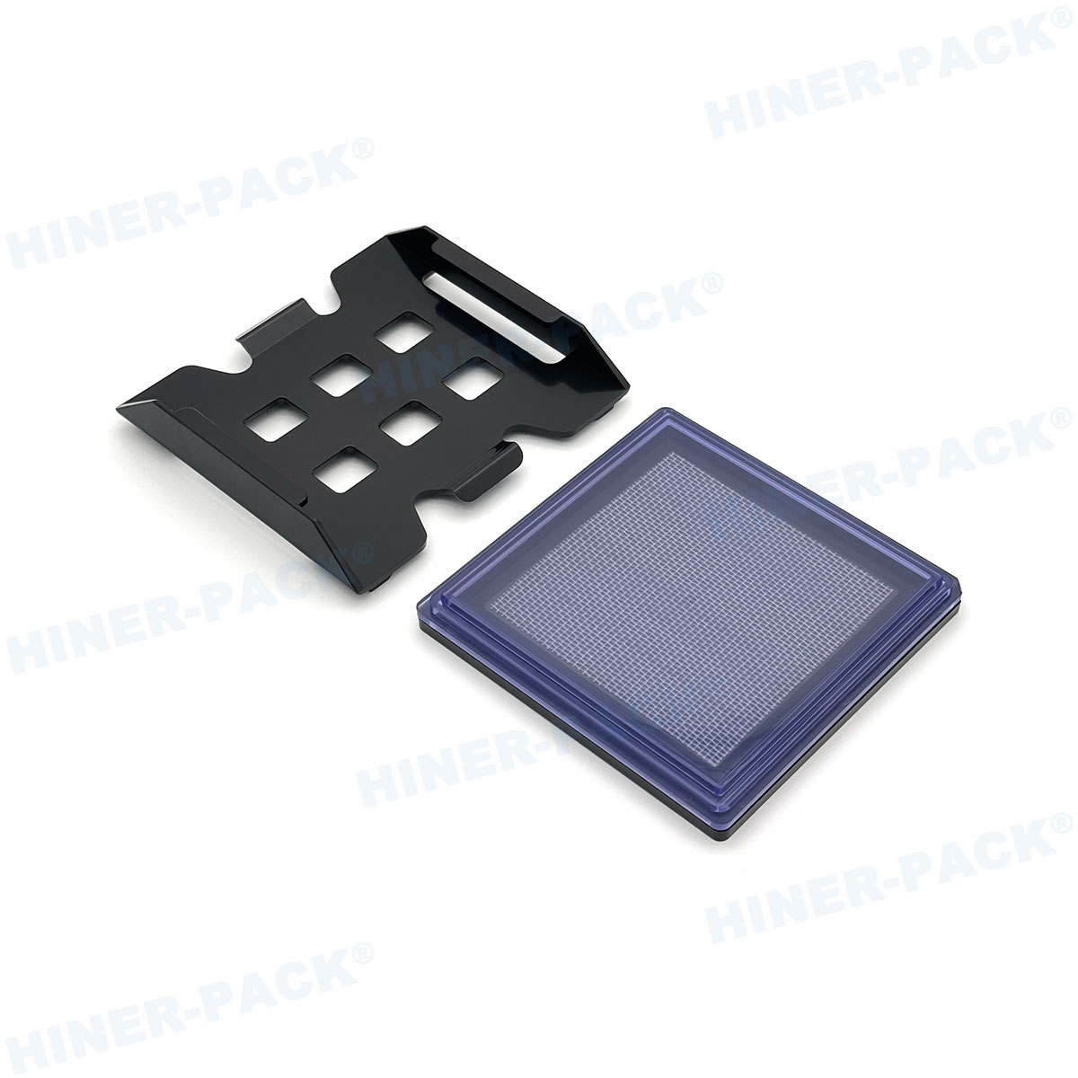
A waffle pack for semiconductors, often called a chip tray or matrix tray, is a specialized container designed to hold individual bare dies. They get their name from the grid-like pattern of pockets that resembles a breakfast waffle.
Each pocket holds one specific unit. The pockets match the dimensions of the die, ensuring a snug fit that restricts movement. This segregation prevents chips from colliding with one another during transit.
Most trays adhere to standard industrial sizes, such as 2-inch or 4-inch square formats. This standardization allows them to fit perfectly into automated pick-and-place machines.
The design typically includes:
The Tray: The main body with cavities.The Lid: A cover to keep chips contained.The Clip: A locking mechanism to hold the lid and tray together.
Manufacturers mold these trays with high precision. The tolerance levels are strict because even a slight deviation in pocket size can cause a pick-up error in automated assembly lines.
Why You Need a High-Quality Waffle Pack for Semiconductors
You might wonder why you cannot simply use generic packaging. The answer lies in the microscopic sensitivity of semiconductor components.
Physical ProtectionBare dies are incredibly brittle. A waffle pack for semiconductors provides a hard shell that absorbs impact. The pocket design ensures that the delicate edges of the silicon do not touch the walls forcefully.
ESD ProtectionStatic electricity is the silent killer of electronics. High-quality packs utilize conductive or static-dissipative materials. This creates a Faraday cage effect around the chips, shielding them from external static fields.
Automation CompatibilityModern fabrication plants rely on speed. Robots need to locate chips at exact coordinates. A precise waffle pack for semiconductors guarantees that every die sits exactly where the machine expects it to be.
CleanlinessContamination leads to device failure. These trays undergo manufacturing in cleanroom environments to ensure they are free from dust, oils, and outgassing particles.
Key Materials Used in Waffle Pack Manufacturing
Selecting the right material is critical. The material determines the tray's physical strength, temperature resistance, and electrical properties.
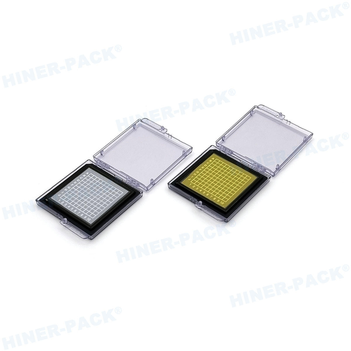
Conductive Black PlasticThis is the most common material for a waffle pack for semiconductors. Manufacturers add carbon powder or fiber to the polymer matrix.
Surface Resistivity: Typically between 10310^3103 and 10510^5105 ohms/square.Function: It drains charge away instantly.Best for: Chips highly sensitive to voltage spikes.
Antistatic/Dissipative MaterialThese trays are often clear or tinted. They allow operators to inspect the contents without opening the pack.
Surface Resistivity: Typically between 10610^6106 and 101110^{11}1011 ohms/square.Function: It prevents charge buildup but discharges it slowly to avoid a spark.Best for: Visual inspection requirements.
Non-ESD MaterialsStandard ABS or Polystyrene is rarely used for active silicon dies because they generate static. However, they might serve for mechanical parts or non-conductive ceramic components.
Suppliers like Hiner-pack offer various material grades to match the specific sensitivity of your components.
Waffle Pack for Semiconductors vs. Gel Paks
Industry professionals often debate between using waffle packs and Gel Paks (VR trays). Both serve similar purposes but work differently.
Waffle Packs
Mechanism: Physical pockets hold the die.Volume: Best for high-volume production.Cost: Generally more cost-effective per unit for standard sizes.Automation: faster for pick-and-place equipment.
Gel Paks
Mechanism: A sticky membrane holds the die in place.Volume: Best for low-volume, prototyping, or broken wafers.Cost: Typically higher.Versatility: Can hold mixed sizes in one tray.
If you are running a production line with thousands of identical chips, a waffle pack for semiconductors is usually the superior logistical choice. It offers faster throughput and easier stacking.
How to Select the Right Waffle Pack for Semiconductors
Choosing the correct tray requires precise measurements. You cannot guess. You need the exact X, Y, and Z dimensions of your die.
1. Pocket Size (X and Y)The pocket must be slightly larger than the die.
If too tight: The die gets stuck.If too loose: The die rotates or flips (tombstoning).A standard clearance is often around 1 to 3 mils (0.025 to 0.076 mm) larger than the device.
2. Pocket Depth (Z)The depth should protect the die but allow easy removal. The chip should sit below the top surface of the tray so the lid does not crush it.
3. Pocket DesignLook for features like:
Draft Angles: Sloped walls that help the die slide into the center.Relief Holes: Holes in the bottom that allow cleaning fluids to drain or vacuum to hold the tray.Corner Radius: Sharp corners on a tray can stress the die; rounded corners are often better.
4. Vendor ReliabilitySourcing matters. You want a vendor who provides technical drawings and samples. Hiner-pack is known for assisting clients in matching their specific die dimensions to the correct mold, ensuring you do not waste money on incompatible trays.
The Role of Accessories: Tyvek Paper and Clips
A waffle pack for semiconductors rarely works alone. It functions as part of a system.
Tyvek Separator PaperYou place a sheet of lint-free paper, typically Tyvek, between the tray and the lid.
Prevents Movement: It acts as a soft buffer.Prevents Static: Antistatic paper adds another layer of ESD safety.Prevents Sticking: It stops the die from sticking to the plastic lid due to static or humidity.
Foam CushionsSometimes, a thin layer of dissipative foam is placed under the lid to apply gentle downward pressure, keeping the dies seated in their pockets.
The ClipThe clip secures the stack. It must provide enough tension to keep the lid closed but not so much that it warps the tray. Warped trays cause jams in automated handlers.
Proper Handling and Storage of Waffle Packs
Even the best waffle pack for semiconductors cannot protect your chips if handled poorly. Human error is a major cause of yield loss.
Manual Handling
Always use vacuum pens or soft-tip tweezers.Never touch the inside of the pockets with fingers. Skin oils degrade the plastic's ESD properties.Open the tray slowly to prevent lightweight dies from jumping out ("popcorn effect").
Storage ConditionsStore these packs in a controlled environment.
Humidity: Keep humidity moderate. Too dry increases static; too wet allows moisture absorption.Temperature: Extreme heat can warp the plastic.Stacking: Do not stack heavy objects on top of the trays.
Cleaning and ReuseSome companies reuse trays to save costs. However, reuse carries risks.
Wear and Tear: The carbon powder in conductive trays can slough off over time (sloughing).Deformation: Repeated heating and cooling cycles change dimensions.Cleaning: You must use specific ESD-safe detergents.
If you notice burrs or scratches on the tray surface, discard it immediately. The cost of a new tray is negligible compared to the cost of a damaged wafer.
The Importance of Customization
Standard off-the-shelf trays cover many common die sizes. However, semiconductor technology shrinks every year. New distinct form factors emerge constantly.
Custom tooling might be necessary if you have:
Oddly shaped dies (non-rectangular).Thinned wafers (ultra-thin dies).Dies with delicate bumps or wire bonds.
Manufacturers like Hiner-pack can create custom molds. While the initial tooling cost is higher, the long-term savings in reduced breakage and faster processing speeds justify the investment. A custom waffle pack for semiconductors ensures your specific product fits perfectly, every time.
Shipping Considerations for Global Logistics
Sending chips across the ocean requires robust packaging. The waffle pack is the primary unit, but the outer packaging matters too.
Vacuum SealingTrays are usually stacked in groups (e.g., 5 or 10), clipped, and then placed in a Moisture Barrier Bag (MBB).
Desiccant: A packet is added to absorb moisture.HIC: A Humidity Indicator Card shows if the seal failed.Vacuum: Air is removed to prevent the trays from shifting inside the bag.
BoxingThe sealed bags go into padded boxes. This multi-layer approach protects against the rough handling typical of air freight and courier services.
The humble waffle pack for semiconductors plays a massive role in the electronics supply chain. It is the bridge between the wafer fab and the final assembly house. Without these precise, conductive trays, the yield rates of modern electronics manufacturing would plummet.
From choosing the right conductive material to calculating the perfect pocket depth, every detail matters. Ignoring these specifications leads to chipped edges, cracked dies, and ESD damage.
Whether you are managing a large foundry or a specialized testing facility, investing in quality carrier systems is mandatory. Companies that partner with experienced suppliers like Hiner-pack find that their logistics issues decrease significantly. They enjoy better protection, higher compatibility with automation, and peace of mind knowing their silicon is safe.
Make sure you evaluate your current packaging strategy. Using the correct waffle pack for semiconductors is the most cost-effective insurance policy you can buy for your high-value components.
Common Questions (FAQ)
Q1: Can I reuse a waffle pack for semiconductors multiple times?
A1: Yes, you can reuse them, but with caution. You must inspect them for physical damage, warping, or contamination. Over time, the conductive coating may wear off, reducing ESD protection. Most high-reliability sectors prefer single-use to guarantee safety.
Q2: How do I clean a dirty waffle pack?
A2: You should use a cleaning solution specifically designed for ESD plastics, often utilizing deionized water and mild, non-abrasive detergents. Avoid strong solvents like acetone, as they can dissolve the plastic or strip away antistatic properties. Drying must be done in a clean, dust-free environment.
Q3: What is the difference between a waffle pack and a JEDEC tray?
A3: A waffle pack for semiconductors (often 2" or 4") is typically used for bare dies before they are packaged. A JEDEC tray is a larger, rectangular standard tray used for transporting finished, packaged ICs (like BGAs or QFNs). JEDEC trays are too large for handling tiny bare dies effectively.
Q4: Why are most semiconductor waffle packs black?
A4: The black color usually indicates the presence of carbon additives. These additives make the plastic electrically conductive, which is essential for draining electrostatic charges away from the sensitive silicon chips. Clear trays are usually antistatic but not conductive.
Q5: How do I know which pocket size to choose for my die?
A5: You need to measure the length, width, and thickness of your die. The pocket should be approximately 2-5 mils (0.05 - 0.12mm) larger than the die to allow for easy insertion and removal without excessive movement. It is best to consult with a supplier like Hiner-pack to check their standard mold list against your measurements.


