
Semiconductor fabrication demands extraordinary precision, where even microscopic imperfections can render entire production runs useless. As silicon wafers progress through various manufacturing steps, thin-film depositions, and lithographic stages, their transport between facilities becomes a phase vulnerable to physical and chemical damage. To maintain substrate integrity, selecting the correct wafer transport packaging is a necessary step for cleanroom managers and packaging engineers.
Finding a reliable wafer canister for sale requires an understanding of structural materials, environmental contamination factors, and mechanical dampening. Hiner-pack designs and manufactures wafer canisters aimed at addressing these exact demands, ensuring that fragile semiconductor substrates arrive at their destination without degradation.
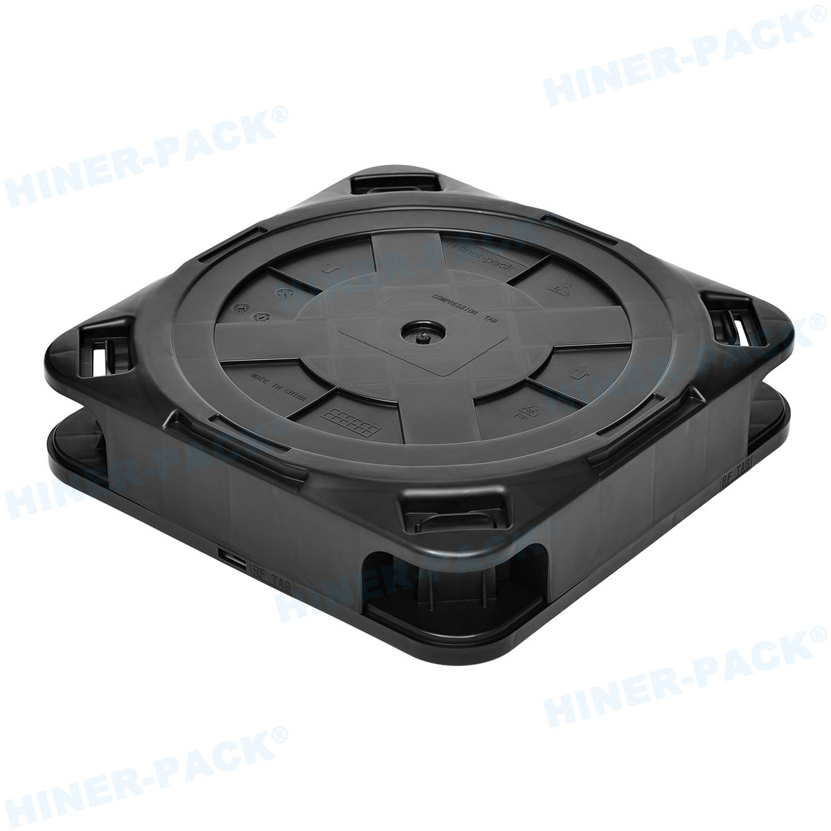
Key Challenges in Wafer Transport and Storage
Silicon, gallium arsenide, and silicon carbide wafers are highly sensitive to physical forces and environmental chemistry. During transit between domestic fabs or international assembly partners, these substrates face several damaging mechanisms that must be suppressed by the packaging architecture.
Particulate Contamination and Outgassing
Microscopic particles are the primary cause of yield loss in semiconductor manufacturing. Standard shipping containers can shed micro-particles due to friction between the wafer edge and the carrier slot. This physical friction generates fine dust that settles on the active surfaces of the wafer.
Chemical contamination is another challenge. Many commercial plastics release volatile organic compounds (VOCs) over time, a process known as outgassing. When these airborne organics settle on a wafer surface, they form a molecular layer that interferes with subsequent gate oxide growth or metallization processes. Specialized packaging materials must exhibit near-zero outgassing properties to preserve surface chemistry.
Electrostatic Discharge (ESD) Protection
Electrostatic charges build up naturally through triboelectric friction during shipping vibration. If the shipping container is made of standard insulating polymers, this charge cannot escape. When a conductive tool or operator approaches the wafer, a rapid electrostatic discharge can occur, melting microscopic pathways on integrated circuits.
To prevent this, the wafer canister must be manufactured using materials that provide static dissipation. These materials allow charges to flow slowly and safely to the ground rather than building up on the wafer surface. Maintaining surface resistivity within a specific range is a key requirement for any safe transport container.
Mechanical Vibration and Shock Mitigation
During logistics, packages experience continuous vibrations from road transport or aircraft engines, along with sudden mechanical shocks from handling. Silicon is inherently brittle, meaning minor mechanical shocks can cause micro-cracks along crystallographic planes. These cracks may not be immediately visible but can lead to catastrophic wafer breakage during thermal processing in the fab.
Material Selection Criteria for a Wafer Canister for Sale
The performance of a semiconductor shipping container depends heavily on its polymer formulation. Engineers must balance physical durability, cost, and cleanliness when reviewing a wafer canister for sale. Hiner-pack focuses on specific polymer grades to meet cleanroom and logistics standards.
Polypropylene (PP) and Polycarbonate (PC) are the most common polymers utilized in this field, each offering distinct mechanical properties:
Polypropylene (PP): Known for excellent chemical resistance and high flexibility. It absorbs impact energy well, making it suitable for dampening external shocks. It is often formulated with conductive carbon additives to achieve anti-static properties.
Polycarbonate (PC): Highly rigid and structurally stable. Polycarbonate provides superior dimensional accuracy, which is necessary for automated handling tools. Its transparent or translucent nature allows for visual inspection of the contents without opening the container.
Conductive Polystyrene (PS): Frequently used for coin-style shippers. It offers high rigidity and excellent ESD shielding, making it a reliable option for shipping individual wafers or small batches.
To achieve the necessary electrical properties, these base polymers are blended with conductive carbon powder or inherently dissipative polymers (IDP). This modification alters the surface resistivity of the container, placing it within the dissipative range ($10^5$ to $10^{11}$ ohms per square), which is the industry standard for safe semiconductor handling.
Structural Design Features of Hiner-pack Wafer Canisters
A high-purity shipping container is more than just a plastic box; it is an engineered protective system. Hiner-pack wafer canisters are designed with multiple integrated features to ensure maximum substrate protection during transit.
A standard configuration consists of four primary components:
The Base: Features a flat, rigid bottom designed to prevent wafer warping. The internal base floor is engineered with minimal surface contact areas to reduce the potential for backside particle generation.
The Cover: Screws or snaps securely onto the base, creating a tight seal that prevents external air and moisture from entering. The cylindrical design distributes external forces evenly around the perimeter.
The Spring Cushion: Placed inside the lid, this compressible component applies gentle downward pressure on the wafer stack. This pressure secures the wafers in place, preventing vertical movement during transport.
The Separator Liners: Non-woven polyester or specialty cleanroom-compatible papers are interleaved between wafers. These liners prevent glass-on-glass or silicon-on-silicon contact, reducing friction and wear.
This multi-layered approach ensures that even when subjected to rough handling, the wafers inside remain motionless and isolated from external contamination.
Standard Dimensions and Fab Compatibility
Modern semiconductor fabrication facilities rely heavily on automation. Human contact with wafers is minimized to prevent contamination. Therefore, shipping containers must adhere to precise dimensional standards to ensure compatibility with fab equipment, such as automated vacuum pick-and-place systems and sorters.
When evaluating a wafer canister for sale, procurement specialists must match the container dimensions with the specific wafer diameters processed in their lines. Common wafer sizes supported by Hiner-pack include:
2-inch (50mm) and 3-inch (76mm) Canisters: Typically used for compound semiconductor substrates, such as Gallium Nitride (GaN) or Indium Phosphide (InP), commonly found in optoelectronic and RF device manufacturing.
4-inch (100mm) and 6-inch (150mm) Canisters: Widely used in MEMS fabrication, power semiconductors, and legacy analog IC lines.
8-inch (200mm) Canisters: Standard for automotive sensors, microcontrollers, and power discrete components. These canisters require high dimensional stability to interface with automated unpackaging tools.
Hiner-pack designs its products to comply with SEMI (Semiconductor Equipment and Materials International) standards, ensuring seamless integration into global automated fab environments.
Evaluating the Long-Term Cost of Wafer Packaging
While packaging is sometimes viewed simply as a shipping cost, experienced procurement managers understand that wafer canisters directly impact overall yield rates. A single damaged 200mm wafer containing finished microchips can easily exceed the cost of thousands of packaging containers. Therefore, focusing solely on the lowest unit price can lead to higher overall production costs due to shipping-related defects.
Investing in high-quality packaging from Hiner-pack minimizes the risk of yield loss from cracked wafers, ESD damage, and particulate contamination. Additionally, many of these robust containers are designed for reuse within closed-loop logistics systems, allowing fabs to clean and redeploy them multiple times, which reduces the per-run packaging cost and minimizes plastic waste.
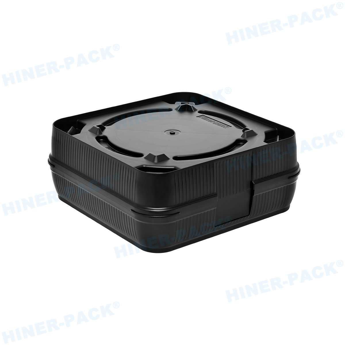
Procurement Considerations for B2B Wafer Shipping Solutions
Selecting a supplier for semiconductor packaging requires a detailed review of their manufacturing capabilities and quality control processes. A reliable partner must operate within a controlled cleanroom environment (typically ISO Class 5 or Class 6) to ensure that the canisters are free from factory-born contamination before they are packed and shipped.
Key parameters to verify with your supplier include:
Outgassing Reports: Request documentation showing low volatile condensable material (CVCM) levels to protect active wafer surfaces from chemical films.
Surface Resistivity Consistency: Ensure that ESD-safe containers maintain uniform resistivity across different batches to prevent localized static build-up.
Traceability: Batch-to-batch traceability is necessary for semiconductor supply chains, allowing rapid root-cause analysis if contamination issues arise.
Hiner-pack maintains rigorous cleanroom manufacturing standards and quality control protocols to meet these strict requirements, providing dependable wafer transport solutions to fabs globally.
Frequently Asked Questions
Q1: What materials are used to manufacture Hiner-pack wafer canisters?
A1: Hiner-pack uses high-purity, cleanroom-grade polymers, including Conductive Polypropylene (PP), Polycarbonate (PC), and Conductive Polystyrene (PS). These materials are chosen for their high mechanical strength, resistance to outgassing, and controlled ESD properties.
Q2: Can Hiner-pack wafer canisters be reused, or are they single-use?
A2: Many of our wafer canisters are designed for multiple uses within closed-loop transport systems. They can undergo standard cleanroom washing and drying cycles without losing their ESD properties or physical dimensions. However, for critical shipping between unrelated facilities, single-use protocols are often preferred to ensure maximum purity.
Q3: How does the internal spring design prevent wafer movement?
A3: The spring cushion inside the lid is engineered to apply a controlled, uniform downward force when the cover is closed. This holds the wafer stack securely against the base, preventing both vertical bouncing and horizontal sliding during shipping vibrations.
Q4: Are Hiner-pack wafer canisters compatible with standard automated handling systems?
A4: Yes, our canisters are designed to comply with SEMI standards. This ensures that their external dimensions, weight distribution, and grip points are compatible with automated vacuum picks, wafer sorters, and handling arms used in modern semiconductor fabs.
Q5: What sizes of wafer canisters does Hiner-pack offer for sale?
A5: We offer a comprehensive range of sizes to accommodate industry-standard wafer diameters, including 2-inch (50mm), 3-inch (76mm), 4-inch (100mm), 6-inch (150mm), and 8-inch (200mm) configurations, with options for custom sizing depending on volume requirements.
Inquire About Hiner-pack Wafer Packaging Solutions
Protecting delicate semiconductor substrates during transit requires high-quality packaging designed for cleanroom performance and physical durability. Hiner-pack provides wafer transport systems engineered to mitigate contamination, ESD, and physical shock.
To request technical specifications, dimensions, material certificates, or a formal quote for our wafer canister for sale, contact our engineering support team directly. We are ready to assist you in selecting the right packaging configuration to protect your semiconductor investments and support your yield goals.














