
In advanced semiconductor fabrication, the integrity of a silicon substrate is highly sensitive to environmental factors. As process nodes shrink below 10nm, the tolerances for micro-contamination, mechanical stress, and electrostatic phenomena become exceptionally narrow. A single microscopic particle or a sudden electrostatic discharge can compromise an entire production run, leading to significant yield loss. Consequently, the transport and storage of processed and unprocessed wafers require specialized packaging solutions. Within this sophisticated supply chain, Hiner-pack operates as an industry provider, fabricating high-purity container systems designed to protect valuable semiconductor substrates during domestic and international transit. Selecting a reliable wafer containers manufacturer is a fundamental step in ensuring yield preservation and maintaining cleanroom compatibility across the supply chain.
Fundamental Challenges in Semiconductor Substrate Transport
Wafers must travel between front-end foundries, testing facilities, and outsourced semiconductor assembly and test (OSAT) partners. During these phases of transit, substrates are exposed to several environmental variables that can degrade their physical and electrical performance.
Particulate Contamination
Airborne molecular contamination and sub-micron particles are persistent hazards. When wafers are subjected to movement inside a carrier, microscopic friction between the wafer edge and the carrier slot can generate debris. A professional manufacturer must utilize wear-resistant polymers that minimize abrasion and particle generation under vibrational stress.
Electrostatic Discharge (ESD) and Triboelectric Charging
Insulative plastics easily accumulate static charges through friction. This static electricity pose two major vulnerabilities:
Attracting airborne particulates from the surrounding environment to the wafer surface.
Causing direct electrostatic discharge that can melt thin-film microstructures on active silicon dies.
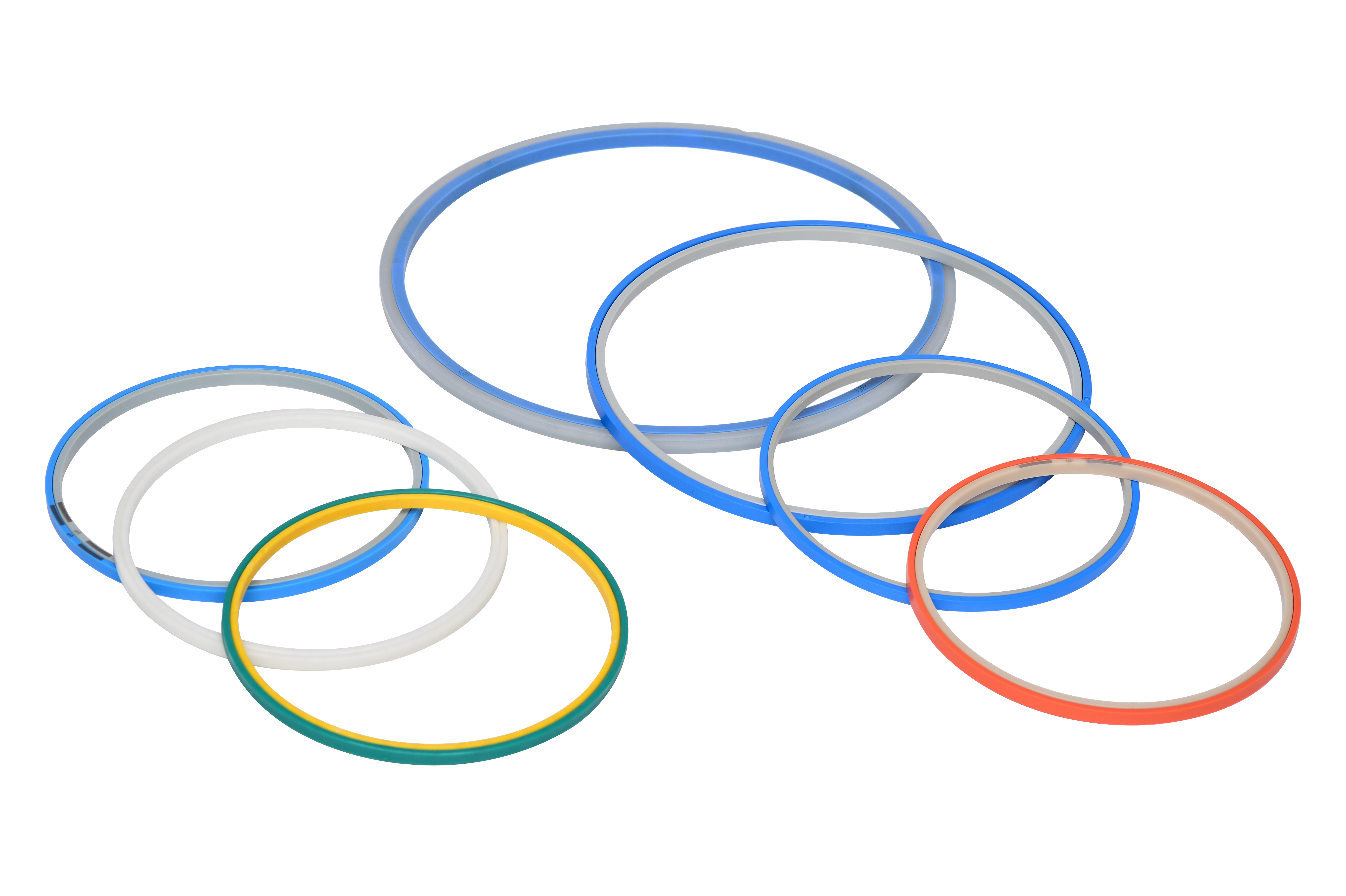
To mitigate these issues, packaging materials must possess specific electrical resistance parameters, typically falling within the static dissipative range of 105 to 1011 ohms per square.
Outgassing of Volatile Compounds
Many industrial plastics release volatile organic compounds (VOCs) over time. In a sealed container, these outgassed molecules condense onto the silicon surface, forming thin chemical films. These films interfere with subsequent deposition and etching steps. High-purity engineering plastics with ultra-low outgassing profiles are required to maintain substrate cleanliness.
Material Science of High-Purity Wafer Shippers
When evaluating a wafer containers manufacturer, material purity must be analyzed. The choice of polymer dictates the container's mechanical stability, ESD performance, and chemical resistance.
Different materials are selected based on the specific phase of wafer handling:
Polycarbonate (PC): Known for high impact strength, dimensional stability, and optical transparency. Carbon-filled or carbon-fiber-reinforced PC is commonly used for structural cassettes and shipping boxes where precise alignment with automated material handling systems (AMHS) is necessary.
Polypropylene (PP): Offers excellent chemical resistance against acids and bases, making it suitable for wet processing cassettes. However, standard PP has lower structural rigidity and thermal resistance compared to engineered polymers, meaning it is typically used for basic shipping jars or coin-style shippers where automated handling tolerances are less demanding.
Polybutylene Terephthalate (PBT): Provides high wear resistance and excellent dimensional stability at elevated temperatures. It is frequently employed in demanding transport systems where mechanical wear at contact points must be minimized.
Polyetheretherketone (PEEK): Reserved for high-temperature processing environments and automated handling cassettes. PEEK exhibits exceptional mechanical properties, chemical inertness, and extremely low outgassing, though its application is usually confined to high-value process steps.
The formulation of ESD additives is also crucial. Standard carbon black compounding provides reliable conductivity but can shed carbon particles under mechanical stress. Advanced manufacturers utilize inherently dissipative polymers (IDPs) or highly carbon-fiber-reinforced matrices that lock the carbon elements within the polymer structure, preventing particulate shedding while maintaining consistent surface resistivity.
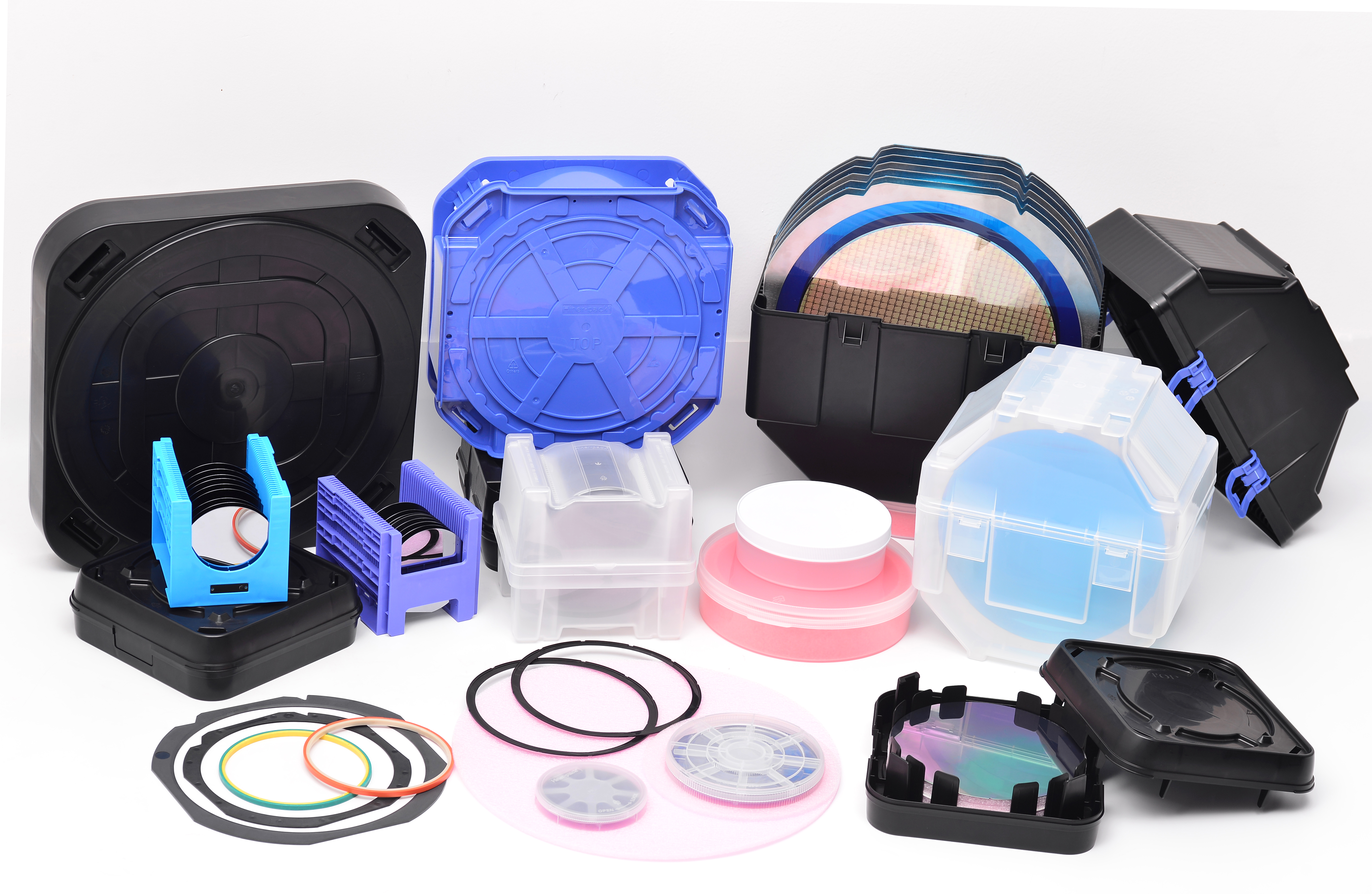
Key Product Architectures in Wafer Packaging
A comprehensive product line is necessary to accommodate different wafer diameters, thicknesses, and processing stages. Industrial wafer containers generally fall into several established configurations:
Coin-Style Wafer Shippers
Designed primarily for the transport of individual, highly thinned, or fragile wafers (such as GaAs, InP, or thin silicon). These containers feature a cylindrical, screw-top or snap-on design. Inside, the wafer is secured by a combination of silicone-free elastomeric cushions and high-purity liners to prevent lateral or vertical movement during shipping.
Wafer Jars and Foam Cushions
For bulk shipping of multiple wafers, wafer jars are often utilized. Wafers are stacked vertically with protective separator sheets (such as cleanroom-grade Tyvek or sulfur-free paper) placed between each substrate to prevent surface scratching. High-density, low-outgassing polyethylene or polyurethane foams are positioned at the top and bottom of the stack to absorb axial impacts during transit.
Horizontal Wafer Shippers
These shippers hold wafers horizontally within a multi-slot internal structure, typically containing 25 slots. The external shell is ruggedized to resist impact, while internal spring retainers apply gentle, continuous pressure to the edges of the wafers, preventing movement within the slots. This configuration is widely used for transport between fabrication stages where automated loading and unloading are not required.
Standard Cassettes and Front Opening Shipping Boxes (FOSB)
For 300mm wafer manufacturing, closed-system transport is standard. FOSBs are designed with precise mechanical interfaces to lock securely onto automated tool load ports. The structural tolerances of these boxes are extremely tight, as robot end-effectors must retrieve and return wafers without mechanical interference. As a specialized wafer containers manufacturer, the supplier must verify compliance with SEMI (Semiconductor Equipment and Materials International) standards for physical dimensions and sensor registration points.
Manufacturing Standards and Cleanroom Protocols
The manufacturing environment of the packaging supplier is just as vital as the design of the container itself. Producing ESD-safe, high-purity polymer containers requires strict cleanroom protocols to ensure that no foreign contaminants are molded into or deposited onto the surfaces of the products.
A reliable production process involves several structured stages:
Precision Injection Molding: Operating within controlled environments to prevent airborne dust from entering the molten plastic feed. High-precision molding machines ensure that dimensional tolerances are held within micrometric limits, preventing structural warping that could damage wafers during robotic handling.
Multi-Stage Ultra-Pure Water Washing: After molding, containers undergo rigorous cleaning using 18 Megohm-cm deionized (DI) water. This process removes surface particles, ionic contaminants, and residual molding lubricants.
Cleanroom Assembly and Packaging: Final assembly of springs, cushions, and latches, followed by primary packaging, occurs inside ISO Class 4 or Class 5 cleanrooms. Products are double or triple-bagged in ultra-clean, vacuum-sealed polyethylene packaging to prevent contamination during storage and transit to the customer's fab.
Facilities operated by Hiner-pack are equipped with automated production lines and testing laboratories. Regular dynamic particle counters, outgassing tests via gas chromatography-mass spectrometry (GC-MS), and surface resistivity meters are employed to confirm that every batch complies with international semiconductor cleanroom requirements.
Evaluating a Global Wafer Containers Manufacturer
For procurement professionals and packaging engineers, establishing a partnership with a qualified supplier involves evaluating several operational capabilities:
1. Custom Engineering Support
Modern semiconductor packaging often involves non-standard wafer thicknesses, custom notches, or specialized substrate materials like glass, quartz, or sapphire. A high-performing wafer containers manufacturer will offer direct engineering support, utilizing CAD modeling and rapid prototyping to develop custom inserts, customized slot configurations, or specialized material blends tailored to specific transport pathways.
2. SEMI Standards Compliance
Interoperability with existing fab automation equipment is non-negotiable. Shippers, cassettes, and boxes must align perfectly with standard vacuum load locks, automated transfer arms, and storage stockers. Verification of compliance with relevant SEMI guidelines (such as SEMI M1, E1.9, and physical alignment specifications) should be provided by the manufacturer.
3. Supply Chain Security
With global semiconductor supply chains facing geographical and operational challenges, a supplier must demonstrate robust raw material sourcing, multi-site production capabilities, and consistent inventory management. This ensures a steady supply of packaging materials, preventing production halts at front-end foundries or back-end packaging houses.
Frequently Asked Questions
Q1: What are the primary differences between ESD-shielding and ESD-dissipative materials in wafer containers?
A1: ESD-shielding materials typically have low surface resistivity (under 105 ohms/sq) and are designed to block external electrostatic fields from penetrating the container. However, they can cause rapid energy transfer if a charged object touches them. ESD-dissipative materials possess a higher surface resistivity (105 to 1011 ohms/sq), which allows electrostatic charges to flow safely and slowly to the ground, preventing sudden energy discharges that could damage sensitive circuit architectures.
Q2: How does outgassing from plastic shipping containers impact silicon wafer yields?
A2: Outgassing occurs when volatile organic molecules escape from the container's polymer matrix. In a sealed wafer shipper, these molecules deposit onto the exposed wafer surfaces. During subsequent high-temperature fabrication processes, such as oxidation, diffusion, or photolithography, these organic residues can act as localized barriers, causing uneven film growth, adhesion failures, or microscopic defects that degrade wafer yield.
Q3: Why are horizontal wafer shippers preferred over vertical configurations for long-distance transport?
A3: Horizontal wafer shippers hold wafers parallel to the ground, supported by continuous slot tracks and secured by spring retainers. This orientation distributes gravity and vibrational forces evenly across the wafer edges. Vertical shipping configurations, while efficient for processing steps, can subject wafers to significant vertical shock during transportation, increasing the likelihood of wafer micro-cracking and chipping at the support points.
Q4: What cleaning protocols should be applied to wafer carriers before reuse in a fab?
A4: Reusable carriers must undergo a systematic cleaning process. This typically involves chemical washing with mild surfactant solutions to remove organic films, followed by multiple rinses with 18 Megohm-cm deionized water to eliminate trace ions and micro-particles. Finally, carriers must be dried using heated, ultra-high-purity nitrogen gas inside an ISO Class 4 cleanroom to ensure no moisture residues remain before reuse.
Q4: How do SEMI standards govern the physical dimensions of wafer shipping systems?
A5: SEMI standards specify precise dimensional tolerances for wafer carriers, including overall width, slot pitch, pocket depth, and the locations of robotic pick-up flanges and registration pins. These standards ensure that containers from any compliant manufacturer can be seamlessly loaded, transported, and unloaded by automated material handling systems (AMHS) and robotic end-effectors across different fabrication tools globally.
Collaborate on Your Semiconductor Packaging Challenges
Protecting delicate semiconductor substrates requires a precise balance of material science, mechanical design, and cleanroom production control. For wafer processing facilities, partner with a wafer containers manufacturer that offers robust, standard-compliant, and customized packaging options designed to preserve yields under demanding transit conditions.
Please contact the engineering team at Hiner-pack to discuss your specific wafer dimensions, material requirements, and cleanliness standards, or to request product samples for evaluation in your facility.


