
The shift toward advanced packaging (fan-out, 3D stacking, chiplet integration) has placed unprecedented demands on wafer handling and transportation. A wafer containers supplier must deliver products that withstand rigorous cleanroom conditions, electrostatic discharge (ESD) control, mechanical shock, and chemical outgassing limitations. Semiconductor backend facilities — from wafer bumping to die attach and molding — require containers that preserve die integrity from the final passivation step through to singulation. This article presents a systematic evaluation framework for procurement and engineering teams, focusing on material properties, dimensional stability, compatibility with automated material handling systems (AMHS), and contamination control metrics. Hiner-pack integrates these principles into its product lines, but the criteria described apply universally to any qualified wafer containers supplier serving ISO 4–6 cleanrooms.
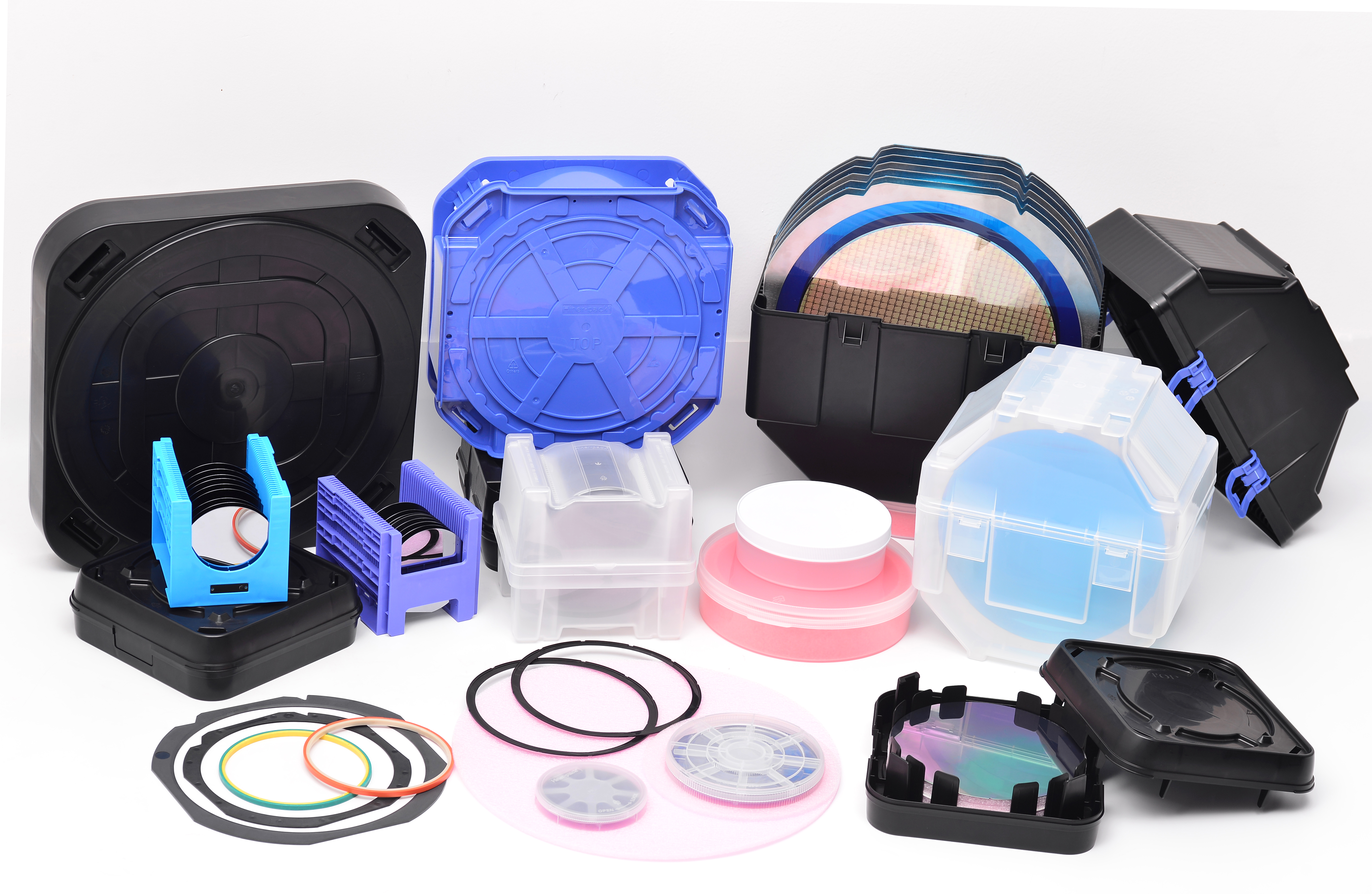
1. Types of Wafer Containers Used in Backend Manufacturing
Different process steps demand different container formats. A single backend facility typically uses four primary categories:
FOUP (Front Opening Unified Pod): Used for 300mm wafers in automated handling; provides hermetic sealing with purge ports. Backend fabs employ FOUPs for bumping and redistribution layer (RDL) processes.
FOSB (Front Opening Shipping Box): Similar to FOUP but designed for inter-facility shipment; includes moisture barrier and impact-absorbent frames.
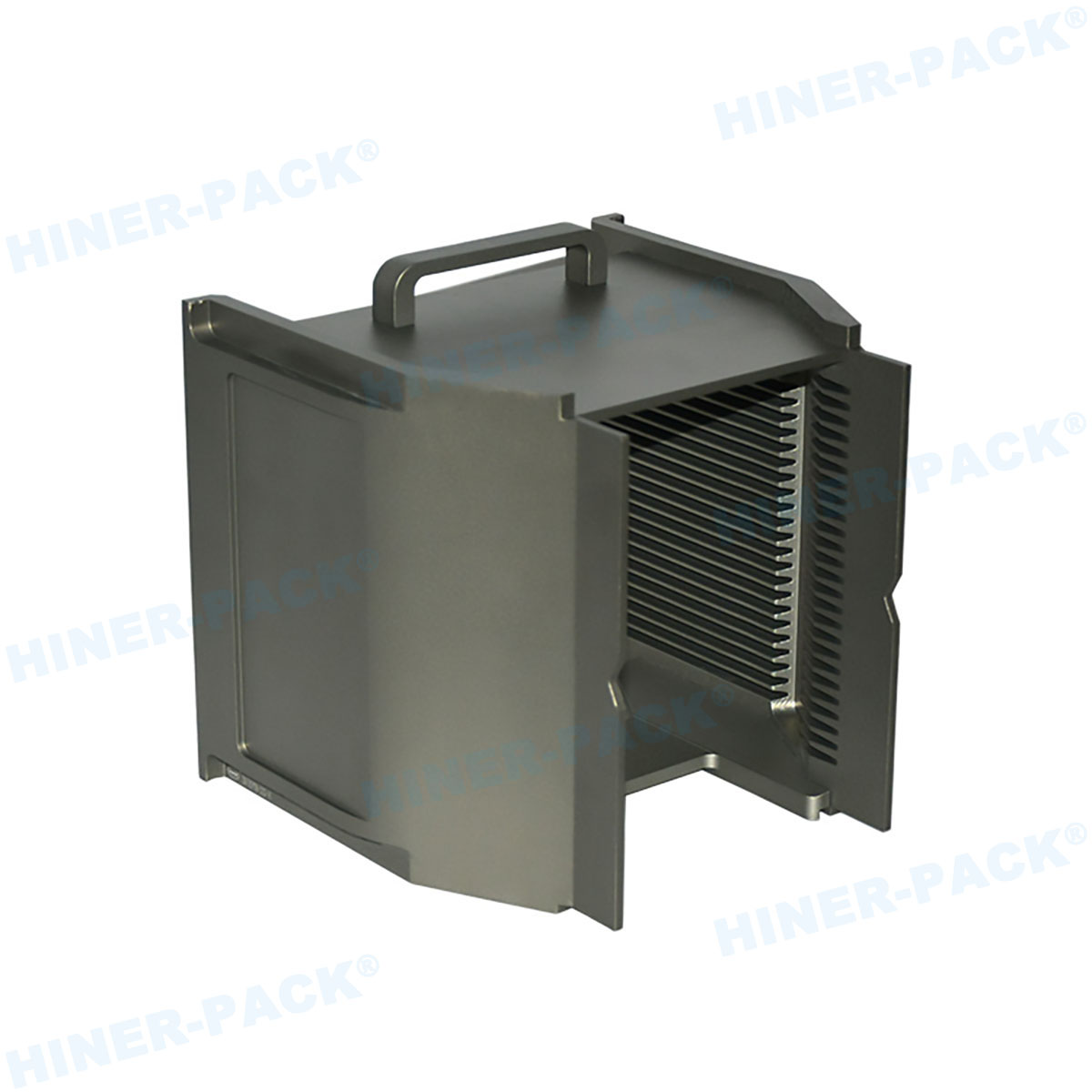
Wafer Shipping Trays (Shippers): Stackable trays for 150mm/200mm wafers, often made from conductive polypropylene or polycarbonate. Common in die banks and outsourced assembly and test (OSAT) facilities.
Single-Wafer Carriers (SWC) or Clamshells: Used for thin wafers (after backgrinding) and sensitive MEMS devices. Provide individual isolation to prevent die-to-die contact.
Selecting a wafer containers supplier that offers all four types under consistent quality management (ISO 9001:2015 + IATF 16949) reduces qualification overhead.
2. Material Science & Contamination Control
Container materials directly influence particle shedding, ionic contamination, and outgassing. The semiconductor industry references SEMI E108 (fluorescing wafer surface contamination) and SEMI E49 (outgassing test methods).
2.1 Base Polymers and Additives
Common substrates include:
Polycarbonate (PC): High clarity, good impact strength, but susceptible to stress cracking under certain chemicals. Used for FOUP windows and shipping boxes.
Polypropylene (PP): Excellent chemical resistance, lower particle generation, but softer surface. Preferred for wafer trays in wet process steps.
PEEK (Polyether ether ketone): High-temperature stability (up to 260°C), ultra-low outgassing. Reserved for FOUP critical components and high-purity applications.
Any wafer containers supplier must provide material certificates (FDA-compliant for medical packaging? No, but SEMI-compliant). Avoid containers with slip agents (e.g., erucamide) or antistatic additives that can migrate to wafer surfaces. Instead, use inherent dissipative polymers (e.g., carbon nanotube-loaded PC) or permanent antistatic agents compounded into the resin.
2.2 Particle Performance Metrics
Containers are tested per SEMI E62 (particle contribution from FOUP) and SEMI E126 (tray particle performance). Acceptable limits:
≥0.1 µm particles added per wafer pass: ≤ 5 particles (for ISO Class 4 environment).
≥0.3 µm particles: ≤ 1 particle per container cycle.
No metallic or fiber contaminants visible under 10x magnification.
Backend processes involving copper pillar plating or solder ball attach are extremely sensitive to metallic ions (Na+, K+, Fe3+). A reputable wafer containers supplier performs ion chromatography (IC) on container extracts, reporting to parts-per-billion levels.
3. Mechanical and Dimensional Integrity for Automation
Modern backend fabs use overhead hoist transport (OHT) and automated guided vehicles (AGVs). Container dimensional tolerances must align with SEMI E1.9 (300mm FOUP interface) or SEMI E47 (200mm tray stack height).
3.1 Critical Dimensional Features
Wafer pocket pitch: ±0.1 mm to prevent wafer edge chipping during insertion/retrieval.
Latch mechanism cycle life: Minimum 10,000 open/close cycles without particle increase.
Flatness of base plate: ≤0.3 mm across the entire footprint to ensure robot end-effector alignment.
Warped containers cause robotic arm collisions, leading to wafer breakage. A wafer containers supplier should provide dimension reports from coordinate measuring machine (CMM) inspection for each production batch.
2.3 (correct numbering) ESD Protection Levels
Surface resistivity: between 10⁴ and 10¹¹ Ω/sq (dissipative range). For backend processes with sensitive thin-film devices (e.g., GaAs, SAW filters), container surface potential must remain below 50V after triboelectric charging. Hiner-pack implements in-mold labeling with embedded conductive grids to achieve consistent ESD performance without coating flaking.
4. Industry Pain Points and Engineering Solutions in Wafer Container Selection
4.1 Wafer Breakage During Manual Handling
Thinned wafers (below 100 µm) after backgrinding are extremely fragile. Standard carriers cause edge cracks when wafers are tilted during insertion. Solutions:
Use carriers with tapered wafer guides (entry angle >15°) and low-friction contact points (PTFE inserts).
Specify single-wafer “JEDEC trays” with full perimeter support rather than point-contact fins.
For 300mm wafers, select FOUP with soft vinyl wafer rests (instead of rigid polycarbonate fingers).
4.2 Moisture Adsorption Leading to Corrosion
Container materials absorb moisture from ambient air (up to 0.2% by weight in polycarbonate). When containers are sealed and stored, moisture desorbs onto wafer surfaces, accelerating aluminum pad corrosion. Solutions:
Use FOSB with desiccant packs or integrated moisture barrier films (aluminum-coated inner liners).
Specify containers made from low-moisture-absorption polymers: cyclic olefin copolymer (COC) or polypropylene instead of PC.
Implement nitrogen purging for FOUP during storage (continuous low-flow N₂ at 5–10 L/min).
4.3 Cross-Contamination Between Different Process Steps
Residues from photoresist, plating solutions, or die attach epoxy can transfer from wafer to container and then to subsequent lots. Solutions:
Use dedicated container sets per product family (color-coding or RFID tagging).
Implement validated cleaning procedures for containers: ultrasonic washing with DI water + non-ionic surfactant, followed by hot air drying (Class 100 environment).
Work with a wafer containers supplier that offers washability test reports (e.g., 100 cleaning cycles without surface degradation).
5. Compatibility with Automated Material Handling Systems (AMHS)
High-volume backend fabs (e.g., OSATs producing 50M+ units/month) rely on stockers, conveyors, and robot arms. Container features for AMHS compatibility include:
Standard kinematic coupling plates (SEMI E15) for precise positioning on load ports.
RFID slot or barcode label area (size and location per SEMI E4).
Magnetic or mechanical interlocks that prevent accidental opening during transport.
A wafer containers supplier must provide 3D CAD models (STEP or IGES) of the container for offline programming of material handling equipment. Many field failures arise from mismatched pick-up points between robot grippers and container handle geometry.
6. Cleanroom and Outgassing Compliance
Backend processes operate in ISO 5–7 cleanrooms with strict airborne molecular contamination (AMC) limits. Container outgassing must not introduce volatile organic compounds (VOCs) that condense on wafer surfaces. Key standards:
SEMI F57: Limits for low-level polymer outgassing using GC-MS (e.g., toluene, benzene, siloxanes < 10 ng/g).
ISO 14644-14: Assessment of suitability for airborne particle cleanliness.
IEST-RP-CC032: Cleanroom compatibility of materials.
Obtain from your wafer containers supplier a certified outgassing report performed by an independent lab (e.g., Intertek, SGS) using dynamic headspace analysis at 60°C. Avoid suppliers who only provide generic material safety data sheets.
7. Lot Traceability and Lifecycle Management
Each container should be marked with a unique serial number (laser-etched 2D Data Matrix code) enabling tracking of:
Manufacturing batch and date.
Cleaning cycle count.
Repair history (replaced latches, cracked corners).
Hiner-pack integrates this into its quality system, providing QR code labels that survive 500+ cleanroom wipe-downs with IPA. For high-reliability applications (automotive semiconductors, medical ICs), traceability down to individual container level is mandatory for root cause analysis of contamination excursions.
8. Long-Term Supply Stability and Engineering Support
Semiconductor fabs operate on multi-year contracts. A wafer containers supplier must demonstrate:
Inventory buffer (safety stock of at least 3 months' consumption).
Secondary tooling availability (molds for each container type) to avoid single-point failure.
On-site application engineering for troubleshooting (e.g., wafer chipping investigation, AMHS integration).
Before qualification, request a supplier audit report covering injection molding process controls (temperature, pressure, cycle time), incoming resin verification (FTIR spectroscopy), and final assembly cleanroom (ISO 6 or better).
Frequently Asked Questions (Wafer Containers for Semiconductor Backend)
Q1: What is the difference between a FOUP and a FOSB when selecting a wafer containers supplier?
A1: FOUP (Front Opening Unified Pod) is designed for within-fab automated transport using OHT systems. It features a sealed door with purge ports and kinematic coupling for load ports. FOSB (Front Opening Shipping Box) is a transport variant with additional mechanical shock protection (double-wall construction or foam inserts) and moisture barrier. FOSB typically does not include purge functionality. For inter-facility wafer shipment, a wafer containers supplier should provide FOSB with validated drop test data (ISTA 2A or 3A).
Q2: How do I verify that a wafer tray will not scratch the backside of thinned wafers?
A2: Request a tribology test report from the supplier. The test uses a representative wafer (with backside coating if applicable) and cycles insertion/extraction 500 times at standard automation speeds. Post-test, inspect the wafer under darkfield illumination for scratch lines. Also, measure the contact area of tray ribs: broader contact pads (≥1 mm width) with polished finish produce lower contact pressure than narrow ribs. Hiner-pack’s trays use elliptical rib profiles with Ra ≤0.4 µm surface finish.
Q3: What documentation should a wafer containers supplier provide for regulatory compliance (SEMI S2/S8)?
A3: For SEMI S2 (environmental, health, and safety), supplier must provide: material flammability rating (UL 94 V-0 or HB), chemical exposure limits (no heavy metals, no brominated flame retardants), and mechanical hazard assessment (no sharp edges, pinch points). For SEMI S8 (ergonomics), container handle design must allow one-handed lifting without exceeding 4.5 kg per hand. Also, supply a REACH and RoHS compliance declaration. Many fabs now also require conflict minerals disclosure (CMRT).
Q4: Can we reuse wafer shipping trays, and how many cycles are typical?
A4: Yes, injection-molded polypropylene trays can be reused if they are cleaned and inspected. Typical reusable cycle life: 20–50 cycles, after which the tray surface may show wear (scratches that trap particles). For critical thin-wafer applications, limit to 10 cycles. The wafer containers supplier should provide a recommended cleaning protocol (e.g., ultrasonic in deionized water + 0.5% Alconox at 50°C, then spin-rinse and N₂ dry). After each cleaning, verify particle performance using a wafer surface scanner (e.g., KLA Surfscan). Avoid reusing trays with visible cracks or discoloration.
Q5: What lead time is typical for custom wafer container designs (e.g., modified pocket dimensions)?
A5: Custom injection molds require 12–16 weeks for tooling (steel or aluminum) plus 2 weeks for first article inspection. However, many wafer containers supplier offer semi-custom solutions by modifying existing tray inserts or using 3D-printed prototypes for low volumes (50–200 units). For production volumes above 5,000 units, hard tooling is necessary for dimensional stability. Always request a dimensional capability study (Cpk ≥1.33) on critical features before mass production.
Q6: How is electrostatic discharge (ESD) performance measured on wafer containers?
A6: Two key metrics: surface resistivity (ANSI/ESD STM11.11) and discharge time (ESD STM12.1). Surface resistivity should be 10⁵–10¹¹ ohms/sq. Discharge time: when charged to ±1000V, the container surface should decay to ≤100V within 2 seconds (relative humidity 12%±3%). Additionally, measure triboelectric charge generated by sliding a wafer across the container ribs — maximum allowable is ±50V. Hiner-pack containers are tested per IEC 61340-5-1 and provide batch test records.
Request for Quotation – Wafer Container Engineering Specifications
For backend assembly and test facilities requiring qualified wafer containers, Hiner-pack provides full documentation including particle test reports, outgassing analysis, and AMHS compatibility drawings. Submit your detailed requirements (wafer diameter, thickness, process type, container format, and annual volume) via the official inquiry portal. Our engineering team will respond within 5 business days with a technical datasheet and sample qualification plan.
Inquiry portal: https://www.waferboxes.com/ — reference “Wafer containers supplier – backend packaging” for prioritized handling.


