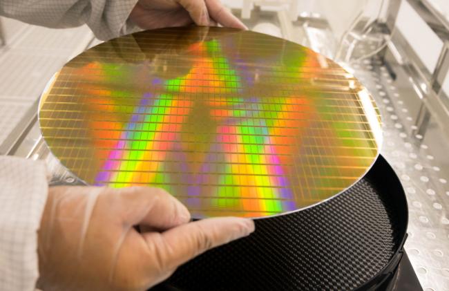
Semiconductor geometries keep shrinking while substrate diameters expand and wafer profiles grow thinner. Inside modern fabs, a single microscopic edge chip or electrostatic discharge (ESD) event can scrap an entire lot of high-value dies.
Automated Material Handling Systems (AMHS) move carriers rapidly between wet benches, metrology tools, and deposition chambers. Outside the fab, inter-facility shipping exposes silicon and compound wafers to relentless shock and micro-vibration.
Working with a technically capable wafer cassettes factory is your strongest defense against preventable yield loss. Since 2013, Hiner-pack has engineered precision carriers built specifically to neutralize static accumulation and mechanical stress.
Are you qualifying new carriers for a production line or troubleshooting transit breakage? Contact our engineering team today to request ESD evaluation samples or discuss custom carrier specifications.
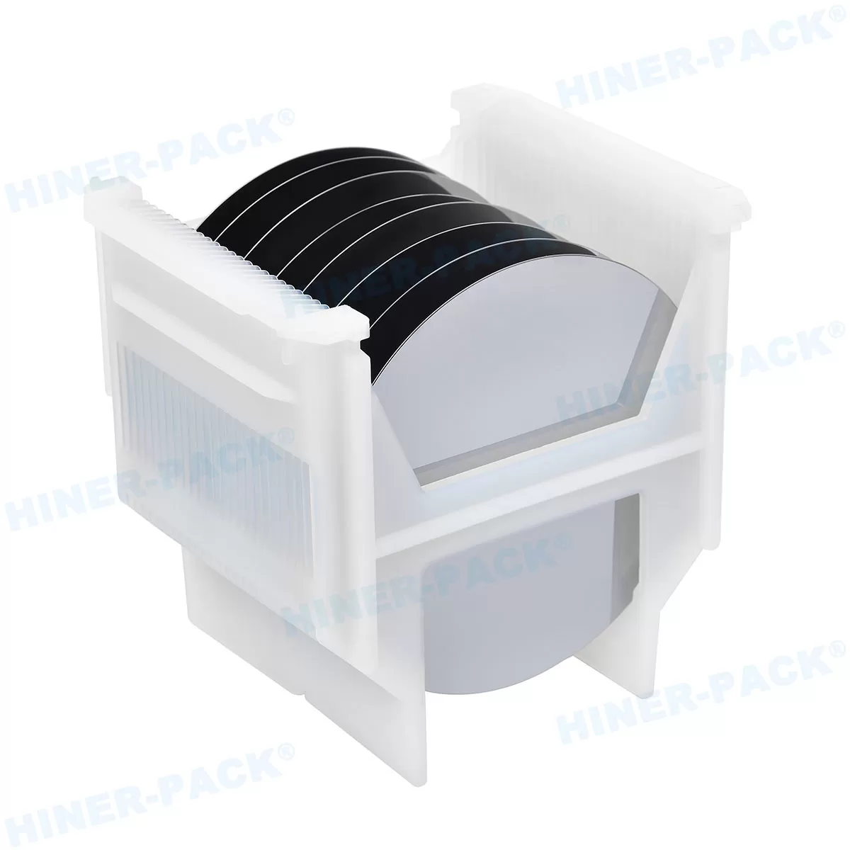
Electrostatic Discharge (ESD) Protection: Stopping Yield Loss at the Polymer Source
Standard injection-molded plastics act as electrical insulators. During high-speed robotic transfers, nitrogen purging, or dry friction, triboelectric charging builds high surface voltages across carrier walls.
This static charge creates two immediate production hazards. First, charged surfaces attract airborne particles straight onto patterned wafer faces. Second, sudden electrostatic discharge events melt nanoscale gate oxides and ruin sensitive integrated circuits.
Joint Polymer R&D and Custom Formulations
Ordinary plastic molders buy off-the-shelf resin pellets and hope for acceptable conductivity. As an engineering-driven wafer cassettes factory, Hiner-pack operates a dedicated polymer material R&D base in partnership with leading domestic universities and research institutes.
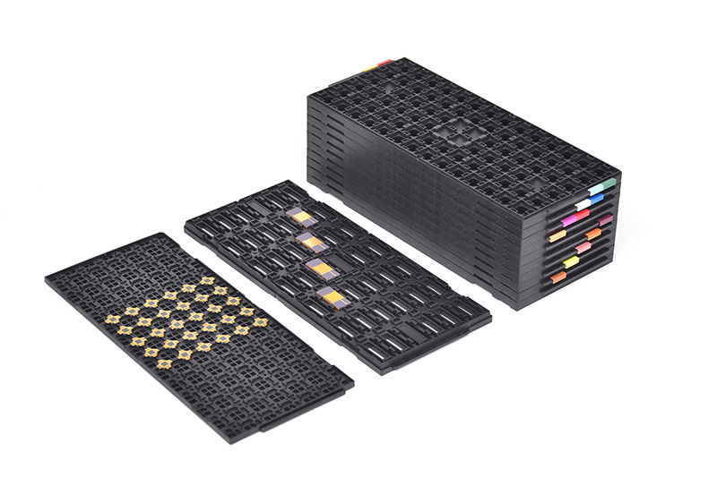
Our polymer scientists develop modified engineering resins tailored specifically for semiconductor handling. Through controlled compounding and specialized processing, we achieve uniform static-dissipative and conductive performance across every pocket, rib, and handle.
- Stable Surface Resistivity: Controlled electrical pathways bleed static charge smoothly to ground without sparking.
- Zero Carbon Sloughing: Proprietary filler dispersion prevents conductive additives from shedding conductive dust onto wafer edges.
- Lot-to-Lot Uniformity: Strict resin verification eliminates resistive dead zones across high-volume manufacturing runs.
Low Outgassing and Chemical Purity
Static control fails if the carrier resin contaminates the wafer microenvironment. Unreacted monomers and plasticizers trapped inside low-grade polymers slowly vaporize inside sealed pods, a contamination mechanism known as outgassing.
Volatile organic compounds (VOCs) condense on copper interconnects, optical lenses, and sensitive passivation layers. Our modified polymer matrices maintain ultra-low outgassing profiles and resist aggressive fab solvents.
Every ESD-safe wafer carrier we produce isolates wafers from airborne molecular contamination (AMC) during multi-week queue times. Your process engineers gain predictable electrical protection without trading away chemical cleanliness.
Vibration and Mechanical Protection: Micron-Level Structural Defense
Static electricity is invisible, yet mechanical shock destroys just as much silicon. As fabs run 200mm and 300mm wafers—or grind substrates down below 100 microns—kinetic energy during transport magnifies stress along the wafer bevel.
Minor warpage in a cassette slot causes robotic end-effectors to strike wafer edges during insertion. During air freight or truck transit, unmitigated micro-vibration induces chatter between the wafer and slot wall, creating micro-cracks and back-side scratches.
Precision Molding for Automated Wafer Handling
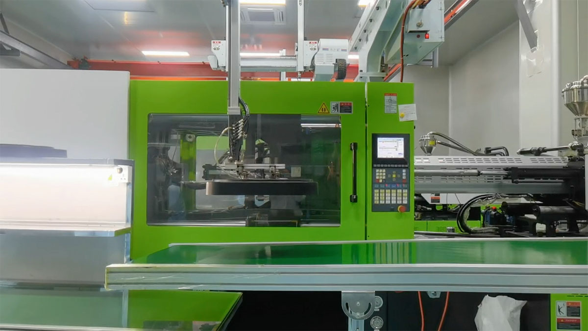
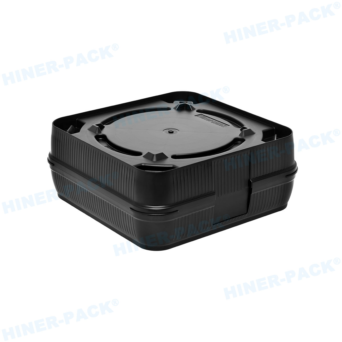
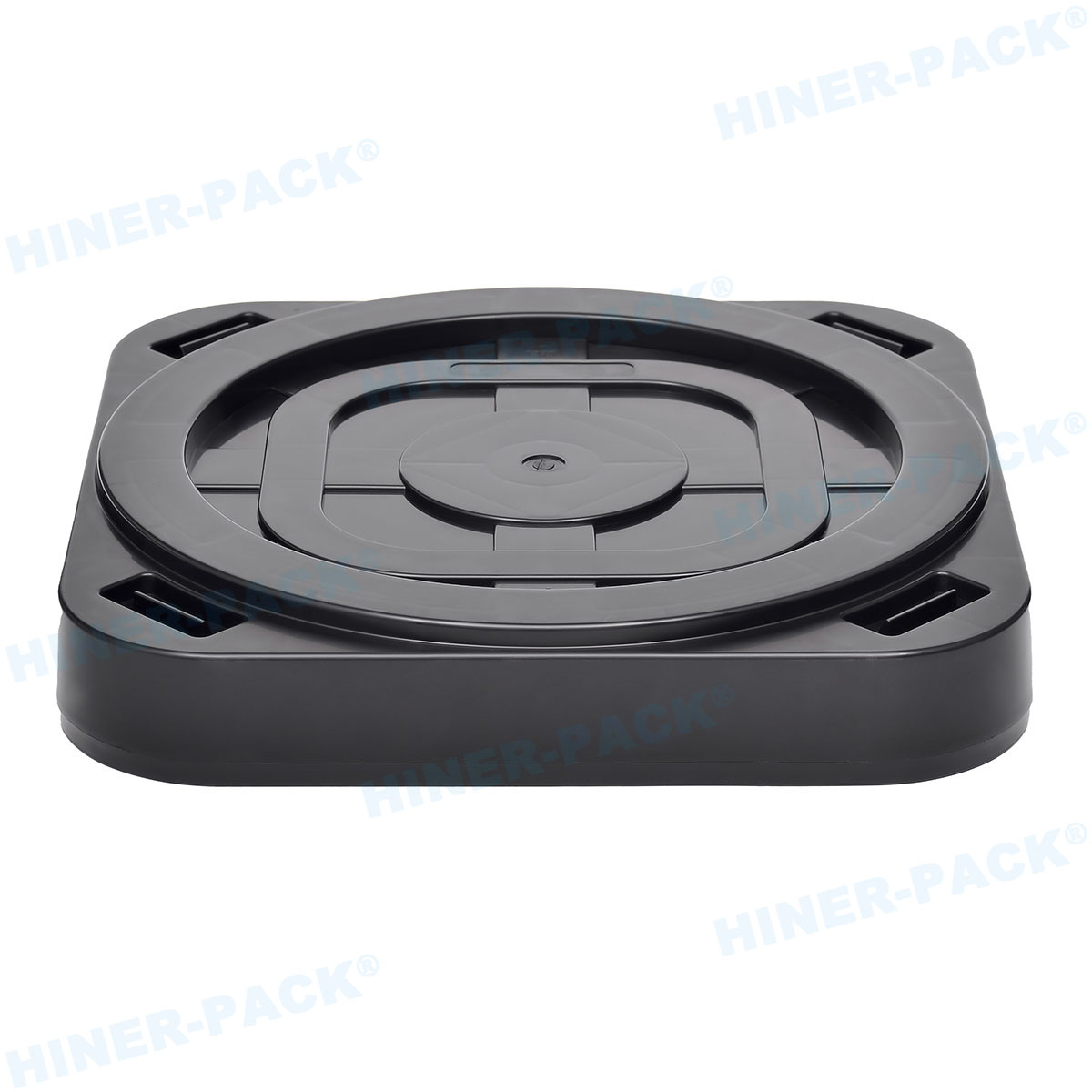
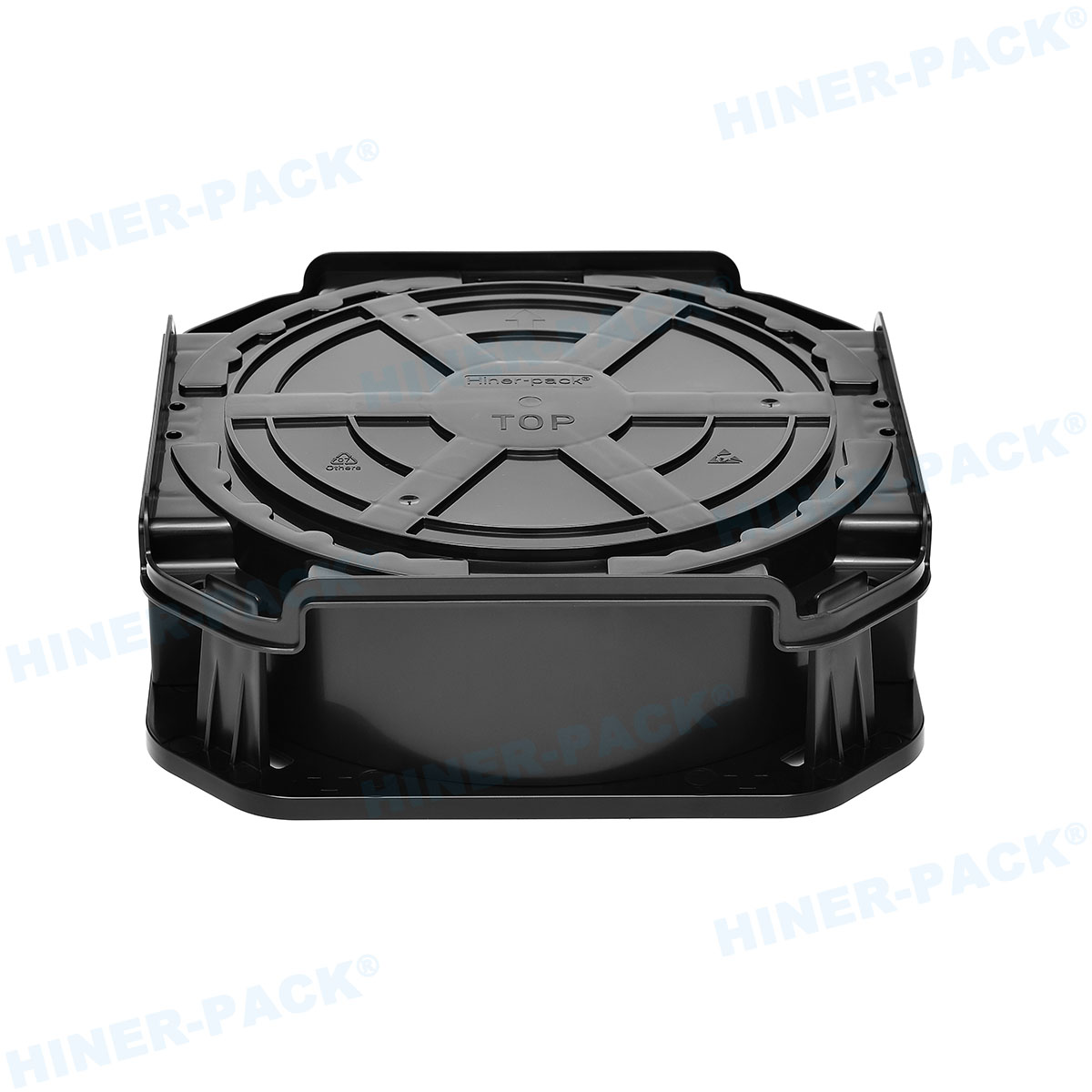
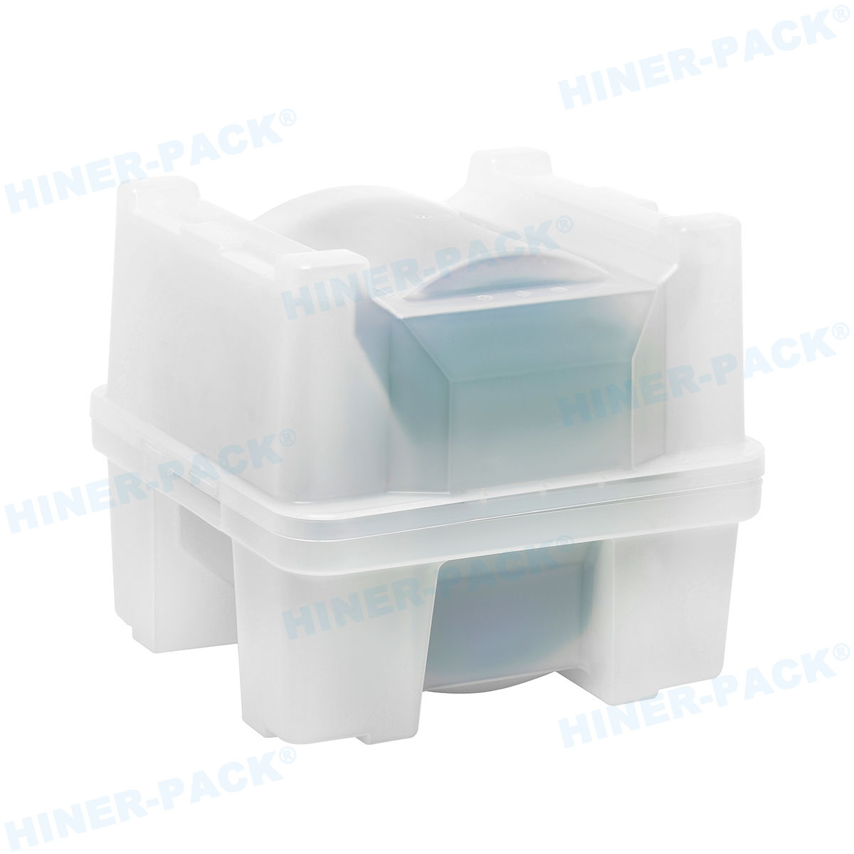
At Hiner-pack, advanced mold fabrication and high-precision injection molding machines enforce tight geometric tolerances. We engineer our Wafer Carrier Series to hold exact slot pitches and flat baseplanes across repeated thermal cycles.
- Ultra-Smooth Slot Geometry: Mirror-polished pocket ribs cut sliding friction as wafers enter and exit the cassette.
- AMHS Alignment Accuracy: Rigid sidewalls and precision locating features guarantee repeatable docking on automated load ports.
- Secure & Stable Wafer Handling: Reinforced structural ribbing eliminates cassette flex when robotic arms lift fully loaded 25-wafer lots.
Reliable automated wafer handling depends on predictable cassette dimensions. By controlling mold shrinkage and post-molding cooling rates, our factory keeps tool alarms and wafer drop incidents near zero.
Shock Absorption for Inter-Fab and Global Transit
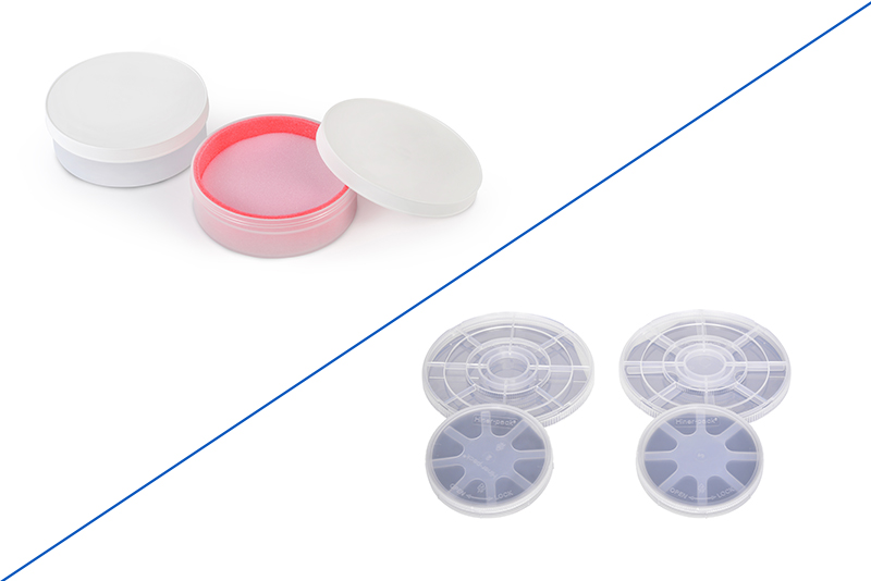
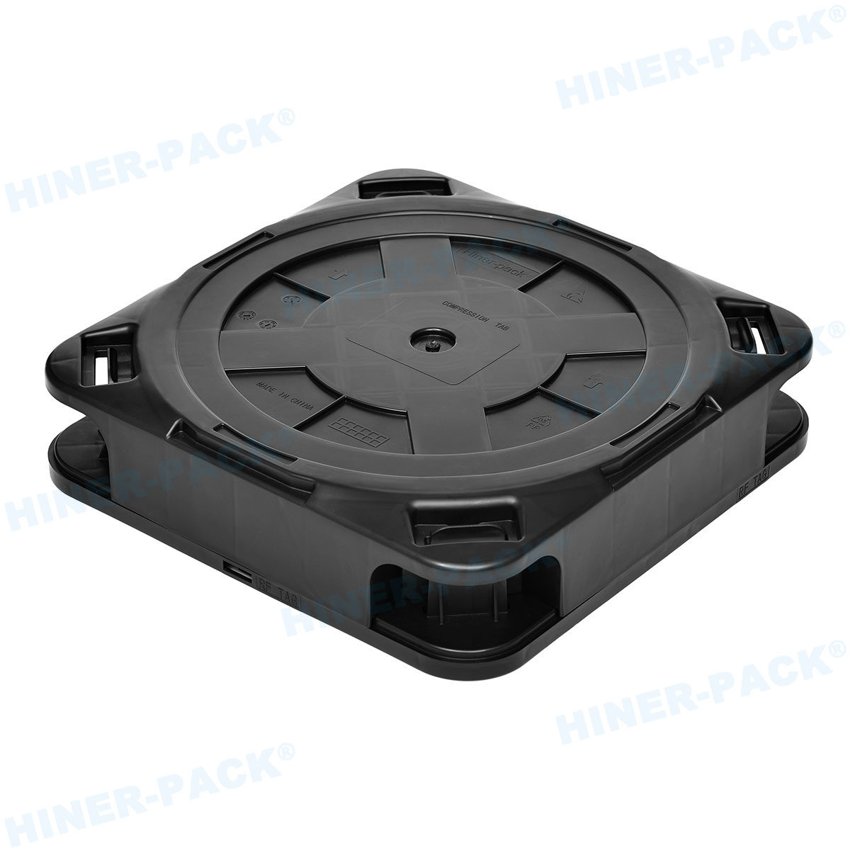
Shipping bare, bumped, or patterned wafers between foundries and OSAT facilities requires more than a rigid plastic box. Paired with our Wafer Shipper Accessories, each carrier acts as a multi-layer mechanical suspension system.
Custom retainer rings, interlocking cushions, and vibration-damping canisters absorb high-frequency road resonance and accidental drop impacts. Following rigorous NIST semiconductor metrology benchmarks for dimensional stability, our assemblies deliver Superior Wafer Protection across global supply chains.
Working directly with an experienced wafer cassettes factory ensures your shipping inserts match exact wafer diameters and thicknesses. Whether you ship fragile silicon or hard silicon carbide (SiC) substrates, engineered damping eliminates transit chipping.
Cleanroom Compatibility and Full-Lifecycle Verification
Precision geometry means very little if a carrier sheds particles inside a Class 10 or Class 100 cleanroom. Out-of-the-box cleanliness separates a dedicated semiconductor wafer cassettes factory from general industrial plastics vendors.
High-Standard Cleanroom Cleaning Line
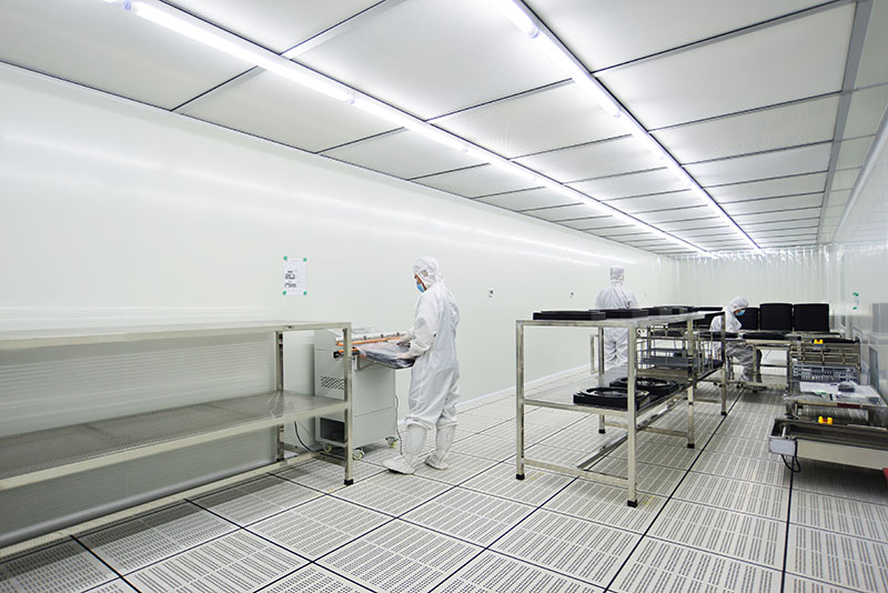
Every cleanroom wafer cassette built at Hiner-pack enters our dedicated cleanroom cleaning production line prior to final packaging. Multi-stage ultrasonic baths and heated ultra-pure deionized (DI) water rinses strip away microscopic debris and trace mold residues.
HEPA-filtered hot air drying chambers remove moisture rapidly without generating fresh static charges. Technicians inspect and double-bag each carrier in vacuum-sealed cleanroom pouches immediately off the drying line.
This verified Cleanroom Compatibility lets your fab team introduce new carriers straight into production zones. You avoid bottlenecks at internal wash stations and accelerate line qualification.
Laboratory Testing and Reusable Cost Economics
Hiner-pack backs every shipment with full-suite laboratory verification rather than visual spot checks. Our quality assurance engineers operate dedicated diagnostic instruments across three core performance pillars:
- Electrical Resistivity Audits: Multi-point surface resistance and static decay testing across internal slots, sidewalls, and handles.
- Coordinate Metrology: High-accuracy pitch, flatness, warpage, and concentricity measurements verifying seamless robotic compatibility.
- Contamination Screening: Liquid particle counting (LPC) and ion chromatography testing to confirm ultra-clean baseline tolerances.
Single-use wafer packaging inflates fab consumable budgets and generates persistent plastic waste. Our modified engineering polymers retain mechanical flatness and ESD stability across dozens of hot DI wash cycles.
Fab procurement teams gain Reusable & Cost-Efficient Solutions that lower total cost of ownership per wafer move. Durable carrier lifecycles reduce replacement frequency without compromising yield safety.
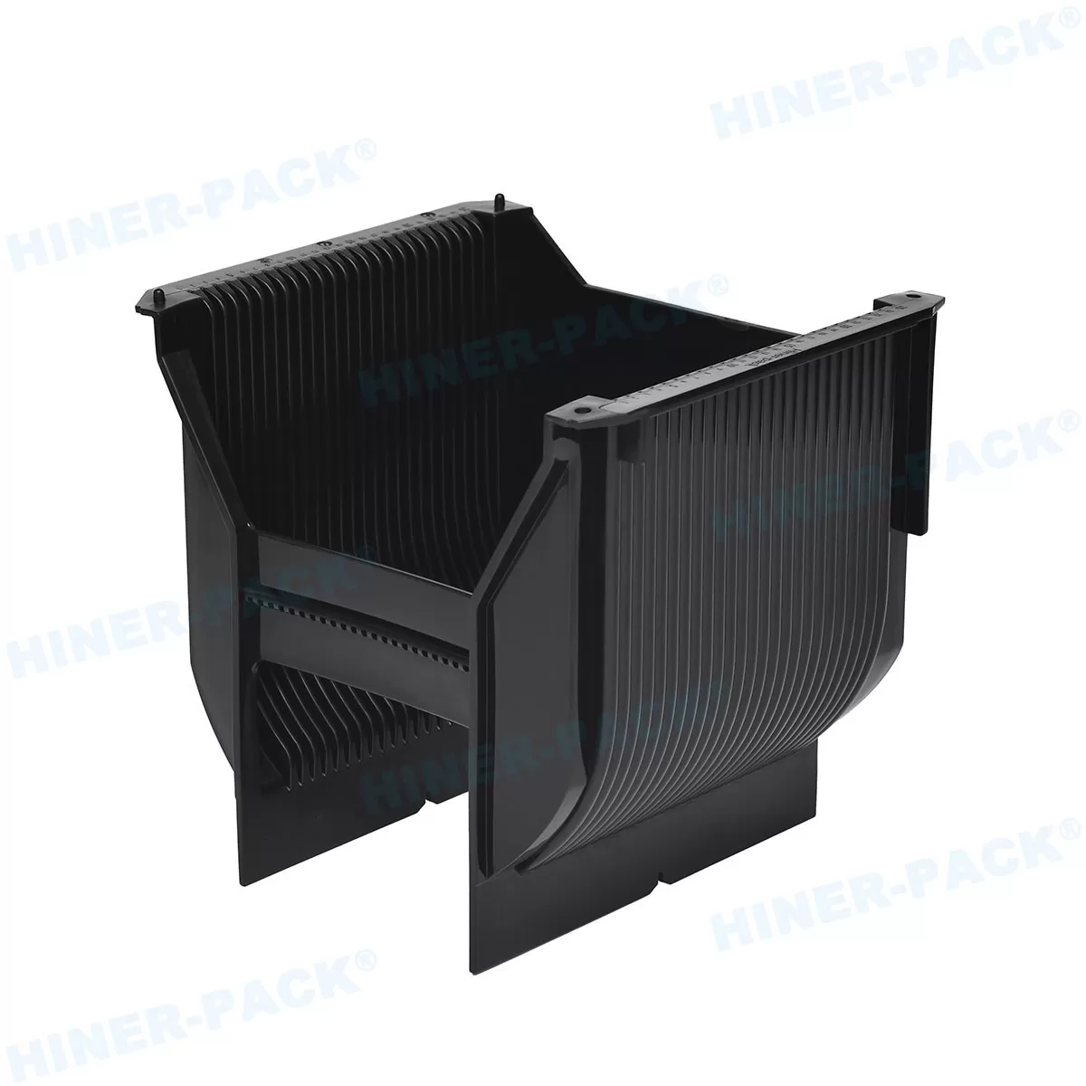
Why Partner with an R&D-Driven Wafer Cassettes Factory?
Sourcing wafer carriers through third-party brokers slows down root-cause engineering and limits customization. When a new ultra-thin process flow or compound substrate enters pilot production, your team needs direct access to material and tooling engineers.
Founded in 2013, Hiner-pack unifies industrial design, polymer R&D, precision molding, cleanroom washing, and global sales within one facility. Our portfolio of invention and utility model patents reflects over a decade of solving real semiconductor handling challenges.
As a vertically integrated wafer cassettes factory, we provide turnkey engineering support alongside comprehensive OEM & ODM services:
- Custom Mold Development: Rapid in-house tooling adapts slot pitches, wafer clearances, and ergonomic flanges for proprietary process tools.
- Targeted Material Engineering: Adjust conductivity bands, thermal deflection limits, or chemical resistance for wet-bench and bake applications.
- Supply Chain Traceability: Direct manufacturing controls guarantee stable lead times, raw resin traceability, and strict batch consistency.
Partnering directly with our technical team puts polymer researchers and precision mold makers on your yield protection roadmap. You gain fast engineering iterations instead of waiting weeks for brokered answers.
Frequently Asked Questions (FAQ)
Q1: What surface resistivity range should an ESD-safe wafer carrier maintain?
A1: Most semiconductor fabs specify surface resistivity between 10^4 and 10^9 ohms/sq, covering conductive to static-dissipative ranges. This controlled window drains triboelectric charges steadily to ground without causing fast, destructive electrical arcs to sensitive dies.
Q2: How does a wafer cassettes factory prevent particle contamination during automated wafer handling?
A2: Particle control combines wear-resistant polymer blends with mirror-finished mold surfaces. Smooth slot geometries minimize abrasion when wafers slide during loading, while ultrasonic DI water cleaning strips away manufacturing dust prior to cleanroom bagging.
Q3: Can Hiner-pack customize carriers for ultra-thin or compound semiconductor wafers like SiC and GaN?
A3: Yes. Through our OEM & ODM customization program, Hiner-pack engineers specialized slot depths, tighter pitch tolerances, and tailored shipping accessories to support fragile, bowed, or non-standard substrates without inducing edge stress.
Q4: Are cleanroom wafer cassettes reusable across multiple fab wash cycles?
A4: Yes. Hiner-pack formulates modified engineering polymers engineered to endure repeated deionized water rinsing, ultrasonic cleaning, and thermal drying cycles. Our carriers maintain dimensional accuracy and stable ESD performance, offering reusable and cost-efficient operation.
Q5: What validation reports should I request before qualifying a new wafer cassettes factory?
A5: Engineering teams should review multi-point surface resistivity maps, dimensional metrology reports, outgassing data, and liquid particle count (LPC) certificates. Hiner-pack provides complete test documentation alongside physical samples for live fab tool trials.
Protect Your Wafer Yield from Fab to Final Delivery
Electrostatic discharge and micro-vibration do not have to erode your semiconductor yield margins. By combining university-backed polymer science, micron-level molding, and cleanroom-validated washing, Hiner-pack protects every wafer through automated handling and global transit.
Whether you are standardizing your Wafer Carrier Series fleet or upgrading Wafer Shipper Accessories for fragile substrates, partnering with an experienced wafer cassettes factory delivers measurable reliability across every lot.
- Request Free Sample for ESD & Cleanroom Testing: Evaluate our dimensional accuracy, surface resistivity, and cleanroom readiness directly on your fab load ports.
- Schedule an OEM/ODM Consultation: Share your wafer thickness, tool interface specs, or transit shock challenges with our R&D engineers for a tailored turnkey solution.
Contact the Hiner-pack engineering team today to start your carrier qualification and safeguard your next wafer production run.