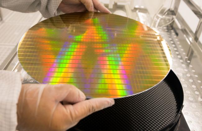
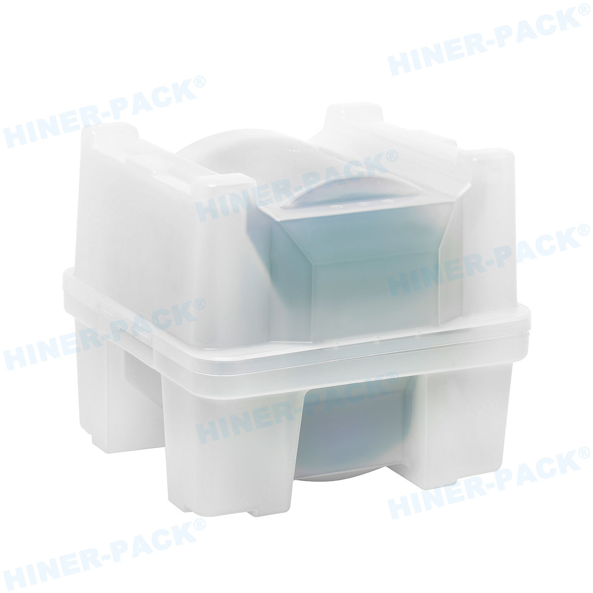
Rapid expansion in 150mm (6-inch) silicon carbide (SiC), gallium nitride (GaN), MEMS, and automotive power chips has placed intense pressure on semiconductor logistics. A single scratch or electrostatic event during inter-fab transit can scrap an entire wafer lot.
To prevent particle contamination, polymer outgassing, and mechanical edge chipping, procurement teams must select a qualified wafer jar supplier. Standard industrial plastic boxes cannot survive cleanroom protocols or long-haul vibration.
This guide breaks down the engineering criteria you should evaluate and compares seven trusted global vendors, starting with manufacturer-direct specialist Hiner-pack. Looking for immediate qualification units? Contact Hiner-pack today to request free 6-inch wafer jar samples or an OEM tooling quote.
5 Engineering Criteria for Selecting a Wafer Jar Supplier
Before issuing an RFQ, fab and OSAT engineers should audit every vendor against strict contamination and mechanical benchmarks. Subpar packaging creates hidden yield losses down the line.
1. Virgin Polymer Purity and ESD Protection
Wafers require containers molded from virgin, high-purity resins with zero recycled fillers or volatile odors. Low outgassing prevents organic haze from forming on polished or epitaxial wafer surfaces.
For sensitive IC devices, containers must also provide controlled static dissipation or conductivity. Verify that your vendor's materials align with international electrostatic protection standards such as IEC 61340-5-1:2024.
2. Cleanroom Compatibility and Wafer-Ready Cleaning
Molding a container is only half the job. A capable wafer jar supplier operates dedicated cleanroom washing lines and inspection equipment to remove submicron particulates before double-bagging.
Ask suppliers whether their jars ship wafer-ready for controlled environments compliant with ISO 14644-1 cleanroom classifications.
3. Physical Cushioning and Accessory Synergy
A rigid jar body needs internal stabilization to absorb shock during air and truck freight. Evaluate whether the vendor supplies matched Wafer Shipper Accessories, including:
- Cleanroom-grade antistatic foam liners that prevent lateral shifting.
- Top and bottom foam cushions to absorb vertical drop impacts.
- Low-lint interleaf paper discs or ring separators to stop wafer-to-wafer abrasion.
4. Reusability and Total Cost of Ownership
Single-use packaging drives up consumables spending and cleanroom waste. High-impact polymer designs allow a reusable wafer shipping container to complete multiple closed-loop trips between foundries and OSATs after recleaning.
5. Existing Mold Library and OEM/ODM Speed
Compound semiconductor wafers often vary in diameter, thickness, and bow tolerance. Partnering with an OEM wafer jar manufacturer that maintains a large catalog of existing molds cuts tooling lead times and upfront NRE costs.
7 Best Wafer Jar Suppliers for Chipmakers & OSATs
The following seven companies serve global semiconductor fabs, substrate producers, and outsourced assembly and test facilities. We evaluated them on material engineering, cleanroom readiness, customization agility, and supply model.
1. Hiner-pack — Best Manufacturer-Direct & Turnkey OEM/ODM Wafer Jar Supplier
Founded in 2013, Hiner-pack is a national high-tech enterprise and pioneer in semiconductor carrier R&D. The company designs, develops, manufactures, and sells automated handling, carrying, and transport solutions for wafer fabrication and IC packaging.
Unlike trading intermediaries, Hiner-pack operates a joint polymer material R&D base with leading domestic universities and research institutes. Its engineering team masters specialized semiconductor polymer compounding and holds multiple invention and utility model patents.
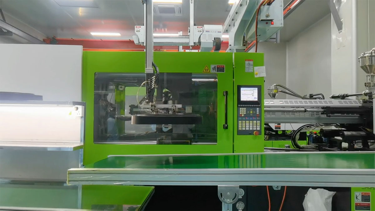
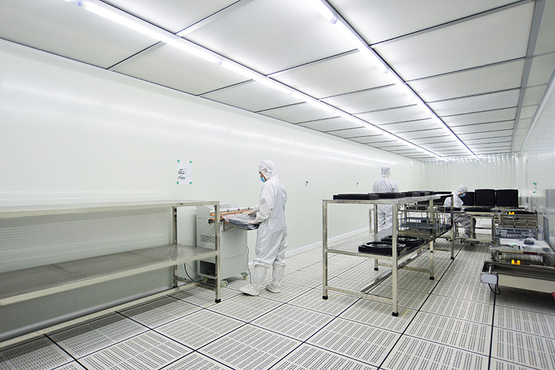
Every production run takes place in facilities equipped with precision mold-making machinery, automated injection molding lines, high-standard cleanroom washing systems, and full dimensional and ESD inspection labs. With over 2,000 existing molds, Hiner-pack delivers fast custom wafer carrier molds and turnkey OEM/ODM support.
Core Wafer Jar Solutions & Product Ecosystem:
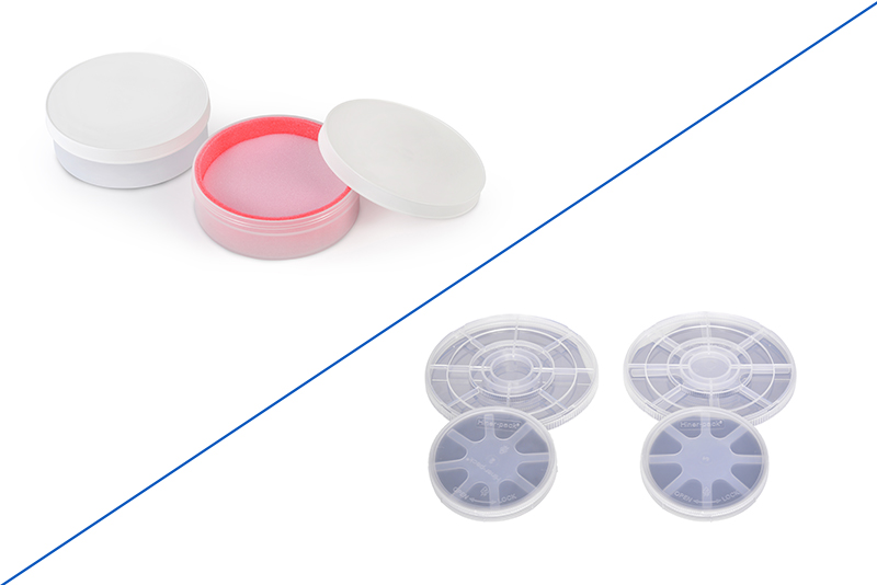
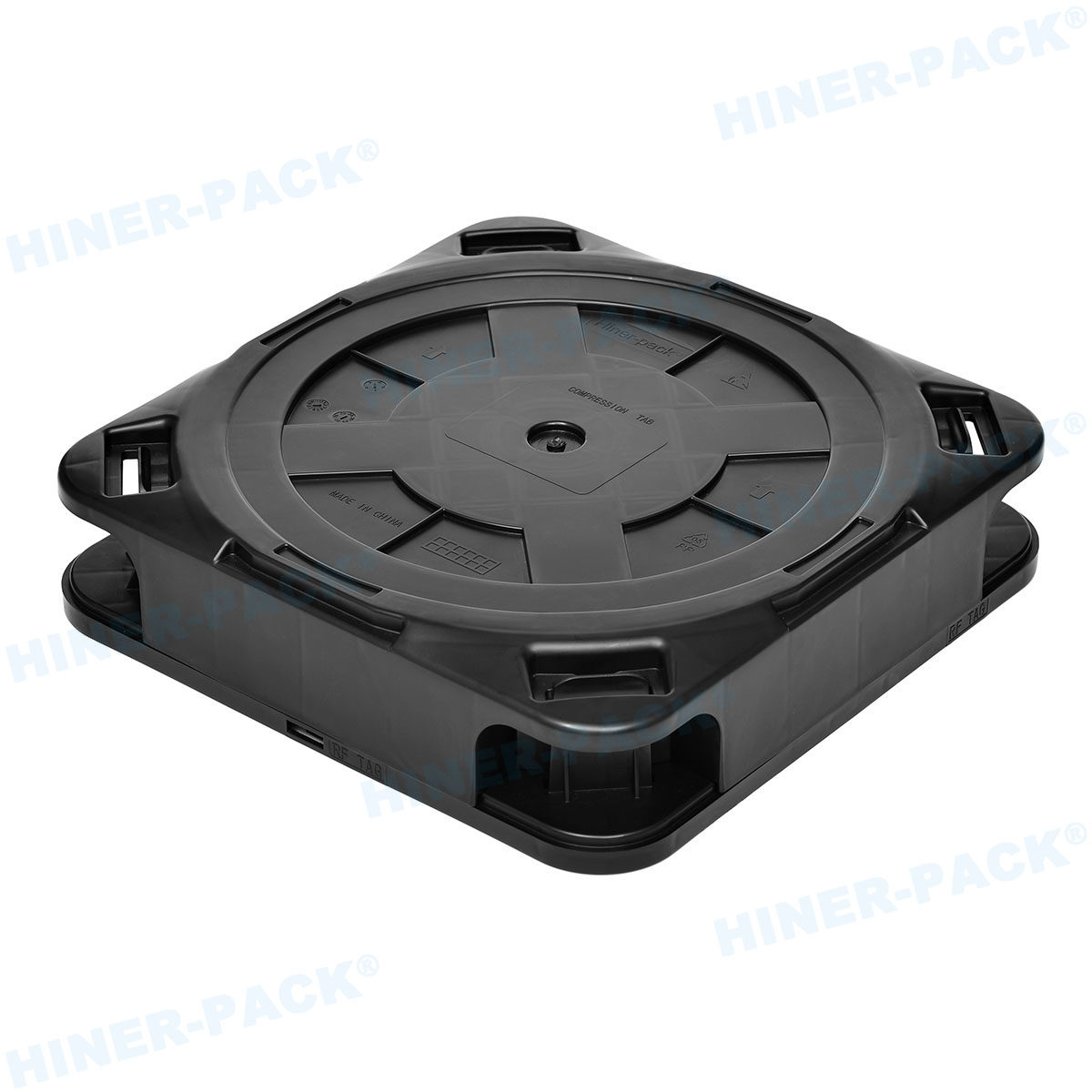
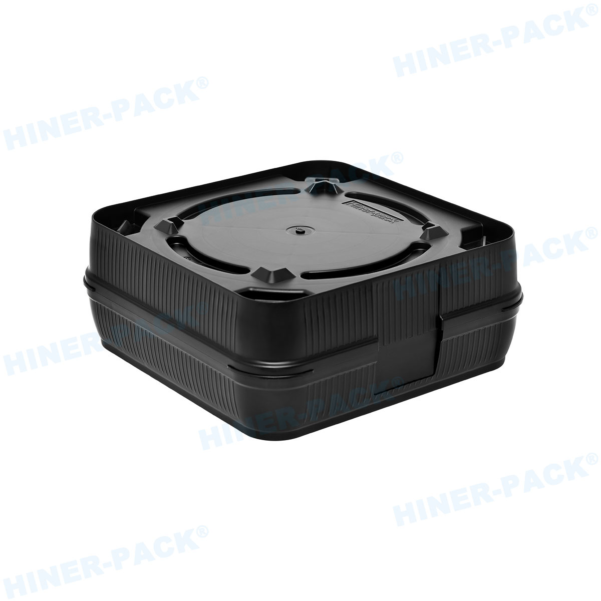
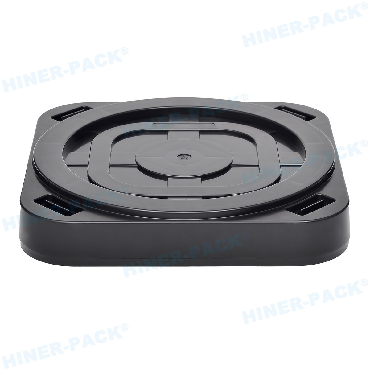
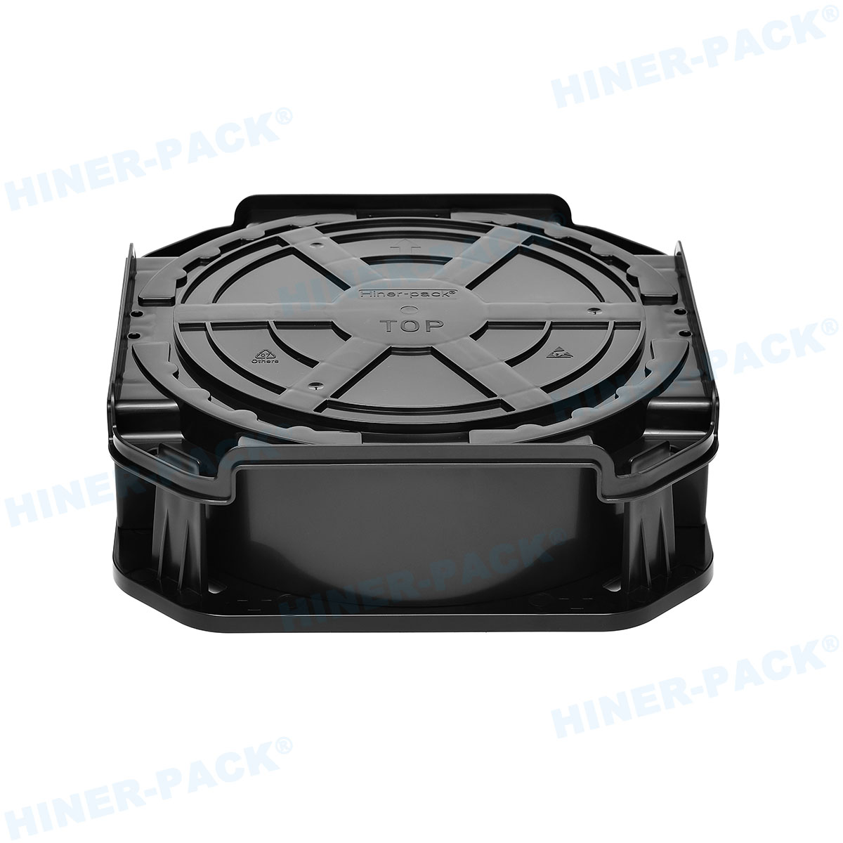
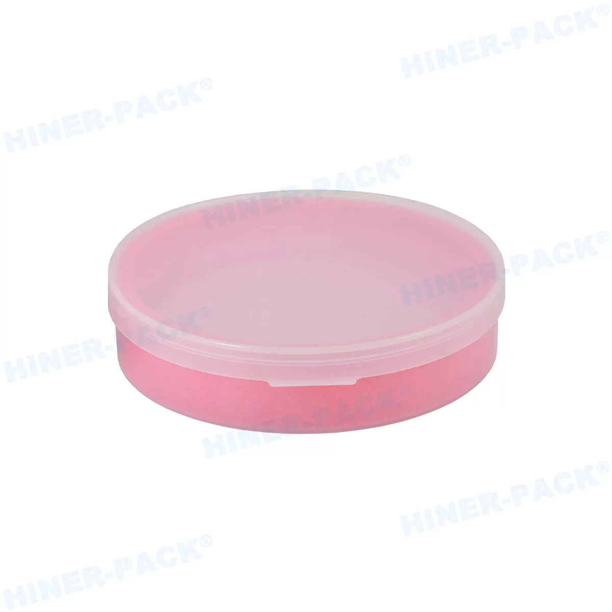
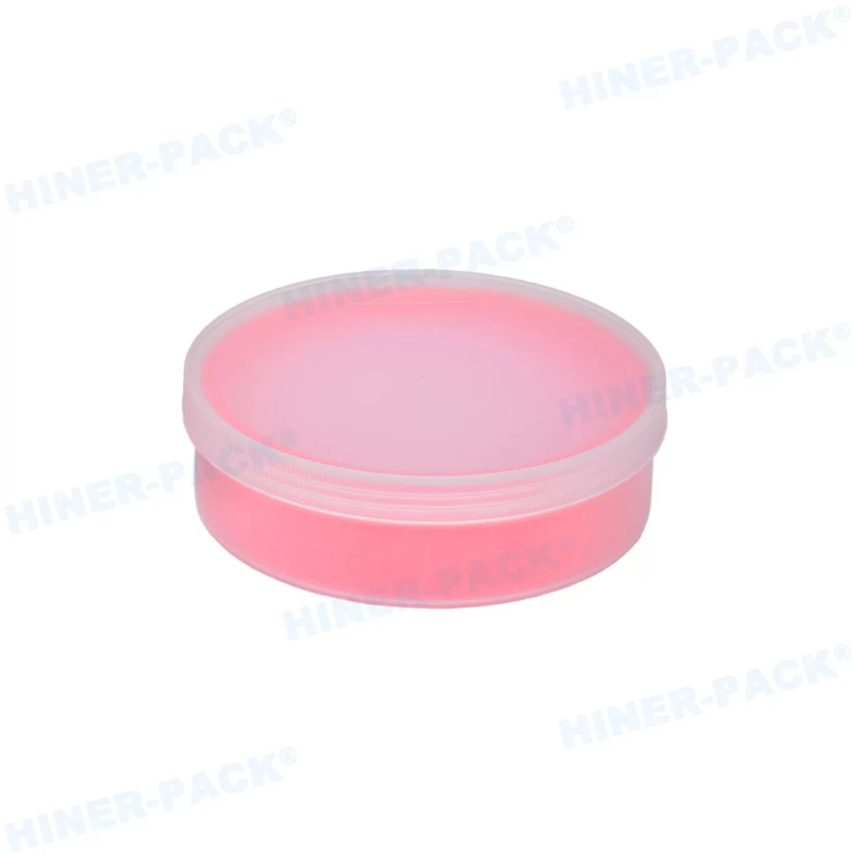
- 6-inch Wafer Jar - Transparent Cover: Engineered for rapid visual inspection, laser mark reading, and barcode scanning without breaking the cleanroom seal—ideal for OSAT incoming QC and R&D lines.
- 6-inch Wafer Jar - White Cover: Built for light-sensitive devices, photoresist-coated substrates, and UV-sensitive compound wafers requiring opaque protection and color-coded lot separation.
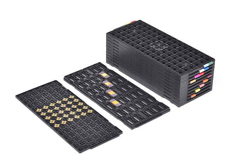
- Complete Semiconductor Packaging Ecosystem: Beyond the 150mm wafer jar lineup, Hiner-pack supplies a full Wafer Carrier Series, Wafer Shipper Accessories, JEDEC Tray/IC Tray, Waffle Pack/Chip Tray, and Gel Box/Vacuum Release Box lines under one roof.
Best For: Global fabs, SiC/GaN foundries, OSATs, and regional distributors seeking manufacturer-direct wafer packaging with high cost-efficiency and rapid OEM/ODM customization.
2. Entegris — Benchmark for High-Volume Automated Fab Handling
Headquartered in the United States, Entegris is a long-standing benchmark in advanced materials handling. Its SmartStack Horizontal Wafer Shippers (HWS) and FOUP lines set strict industry standards for 200mm and 300mm automated fabs.
Entegris excels in contactless perimeter-support shipping for ultra-high-value logic and memory nodes. However, its premium pricing and longer lead times for custom legacy tooling can challenge smaller 150mm specialty fabs.
Best For: Tier-1 300mm IDMs and high-volume foundries running fully automated AMHS load ports.
3. Shin-Etsu Polymer — Material Science & Ultra-Clean Precision Molding
As part of the Shin-Etsu Chemical Group in Japan, Shin-Etsu Polymer brings deep resin synthesis expertise to semiconductor transport. The company is widely recognized for ultra-low-outgassing 300mm FOUPs and Front Opening Shipping Boxes (FOSBs).
Its strength lies in long-term supply agreements with major prime silicon wafer manufacturers. For buyers needing flexible, small-to-medium batch coin stack wafer shipper jars, direct customization options are typically more rigid.
Best For: Prime 300mm silicon ingot and wafer suppliers shipping bulk polished wafers under multi-year contracts.
4. ePAK — Broad Standardized Portfolio for Backend & Wafer Logistics
ePAK offers one of the industry's broadest catalogs of standardized wafer canisters, coin-style shippers, and eJR wafer jars covering 100mm to 300mm diameters. Its global distribution footprint supports both front-end fabs and backend assembly plants.
Procurement teams value ePAK's off-the-shelf availability in conductive and natural polypropylene. Buyers looking for deeply integrated, manufacturer-direct mold co-development on tight regional budgets often compare ePAK against agile Asian OEMs.
Best For: Multinational chipmakers needing standardized multi-size canisters across dispersed global sites.
5. Pozzetta — Specialized Cleanroom Micro-Cleaning & Niche Substrates
Based in Colorado, Pozzetta focuses on photomask compacts, single-wafer coin shippers, and precision micro-cleaning services. Through its dedicated micro-clean division, Pozzetta washes and certifies containers using filtered deionized water inside controlled cleanrooms.
Pozzetta serves North American labs and specialty substrate makers well, especially for small-lot orders and reticle protection. Its catalog leans more toward single-wafer boxes and mask carriers than high-volume multi-stack 6-inch wafer jar tooling.
Best For: North American R&D fabs, photomask shops, and low-volume specialty substrate shipments.
6. SPS-International — European Distribution & Wafer Handling Assembly
Operating out of the Netherlands, SPS-International is an established SEMI member serving European semiconductor manufacturers. The company supplies wafer jars with liners, single wafer clamshell shippers, and automated wafer transfer equipment.
SPS-International stands out for localized European technical support and cleanroom consumables bundling. Because it functions heavily as an integrator and equipment-plus-consumables distributor, pricing reflects multi-tier distribution margins.
Best For: European wafer fabs, MEMS foundries, and research institutes seeking regional fulfillment and handling tools.
7. Miraial — Japanese Precision-Molded Wafer Containers
Miraial Co., Ltd. is a Japanese precision injection molder specializing in 300mm FOSBs, FOUPs, and single-wafer cases. The company pioneered early 300mm shipping box commercialization and operates high-precision vertical molding lines.
Miraial delivers tight dimensional tolerances suited for robotic load-port interfaces in Japan and East Asia. Like other Japanese giants, its focus remains centered on 200mm/300mm automated pods rather than customizable 150mm coin-stack jars.
Best For: Japanese and East Asian automated fabs prioritizing micron-level robotic interface tolerances.
Side-by-Side Comparison of the Top 7 Wafer Jar Suppliers
Use the comparison matrix below to shortlist the right wafer jar supplier based on your wafer diameter, customization volume, and procurement model.
| Supplier | Core Strength / Best For | Key Wafer Jar & Shipper Offerings | OEM/ODM & Mold Capability | Cleanroom & Supply Model |
|---|---|---|---|---|
| Hiner-pack | Manufacturer-direct value, 150mm SiC/GaN & OSATs, turnkey customization | 6-inch Transparent & White Cover Wafer Jars, Shipper Accessories, JEDEC/Waffle Trays, Gel Boxes | Over 2,000 existing molds; rapid in-house OEM/ODM tooling & university polymer R&D | High-standard cleanroom washing lines; full inspection; Manufacturer-Direct & Distributor programs |
| Entegris | Tier-1 300mm automated fabs & high-value IC transport | SmartStack HWS, FOUPs, 150–300mm single & multi-wafer shippers | High engineering capability; higher NRE and longer custom lead times | Ultra-clean global manufacturing; premium Tier-1 pricing |
| Shin-Etsu Polymer | Prime silicon wafer makers & leading-edge nodes | 300mm FOSBs, FOUPs, high-purity polymer wafer cases | Custom resin formulations; focused on large-scale standardized specs | Cleanroom molded in Japan/Asia; long-term enterprise contracts |
| ePAK | Broad standardized backend & multi-size wafer canisters | eJR Wafer Jars, eLX Canisters, coin-style single shippers (100–300mm) | Built-to-order options across standard catalog geometries | Global warehousing; standardized catalog supply |
| Pozzetta | North American specialty substrates & photomask cleaning | Coin-style single shippers, clamshell boxes, reticle compacts | Targeted modifications for thin or niche substrates | In-house DI water micro-cleaning; regional US focus |
| SPS-International | European local distribution & handling equipment bundling | Wafer jars with foam liners, single wafer shippers, transfer tools | Standardized assembly kits; limited custom mold ownership | EU regional inventory; distributor & integrator model |
| Miraial | Robotic load-port dimensional precision | 300mm FOSBs, FOUPs, single wafer cases, PFA cassettes | Precision vertical molding; primarily 300mm automated standards | Cleanroom molded in Japan; focused on automated fab fleets |
Deep Dive: 6-Inch Wafer Jar Transparent Cover vs. White Cover
As semiconductor wafers move from crystal slicing through epitaxy, lithography, and dicing, different process stages demand different enclosure properties. Choosing the wrong lid configuration slows down inspection or compromises sensitive coatings.
Hiner-pack engineers both transparent and opaque cover options for its 6-inch wafer jar family so fabs and OSATs can match packaging directly to process risk.
When to Choose the 6-inch Wafer Jar - Transparent Cover
Select a wafer jar transparent cover when visual traceability outweighs light shielding. Clear lids allow operators and automated optical scanners to verify lot IDs, wafer orientation flats, and stack counts immediately upon arrival.
- OSAT Incoming Quality Control (IQC): Verify wafer quantity and edge condition without unsealing the jar outside an ISO Class 5 zone.
- R&D and Engineering Lots: Speed up manual sorting in pilot lines where engineers frequently inspect substrate batches.
- Clean Bare or Nitride-Passivated Wafers: Ideal for non-photosensitive substrates moving between polishing and metrology stations.
When to Choose the 6-inch Wafer Jar - White Cover
Choose a wafer jar white cover whenever wafers carry light-sensitive layers or require visual lot segregation on the production floor. The opaque lid blocks ambient cleanroom and UV light during storage and transit.
- Photoresist-Coated Wafers: Prevent accidental UV exposure before stepper or scanner alignment.
- Compound Semiconductors (SiC, GaN, InP): Protect sensitive epitaxial and optoelectronic layers from photo-induced degradation.
- Multi-Line Color Coding: Separate prime wafers, test wafers, and reclaim lots at a glance to reduce operator mix-ups.
Maximizing Protection with Matched Wafer Shipper Accessories
Even the strongest wafer shipper jar relies on internal dunnage to achieve zero-defect delivery. Hiner-pack pairs its 150mm jars with precision-cut antistatic foam liners, top/bottom cushion pads, and ultra-clean interleaf separators.
This integrated system eliminates micro-vibrations, prevents surface scratching between stacked wafers, and maintains reliable OSAT wafer handling across international air freight.
Frequently Asked Questions (FAQ)
Q1: What is the difference between a wafer jar (coin-stack shipper) and a single wafer shipper?
A1: A wafer jar—often called a coin-stack wafer shipper—stacks multiple wafers horizontally inside a cylindrical canister separated by interleaf discs and foam cushions. It maximizes packing density and lowers shipping cost per wafer. A single wafer shipper holds only one high-value or fragile wafer in a dedicated clamshell or coin case with edge-only contact.
Q2: Should I choose a transparent cover or white cover for 6-inch wafer jars?
A2: Choose a transparent cover when your team needs to scan barcodes, read laser markings, or visually inspect wafer stacks without breaking the clean seal. Choose a white cover for photoresist-coated wafers, light-sensitive compound substrates, or color-coded production lot separation.
Q3: Are Hiner-pack wafer jars reusable, and how are they cleaned?
A3: Yes. Hiner-pack designs every jar as a reusable wafer shipping container using impact-resistant, high-purity polymers. After each transit cycle, containers can be washed, dried, and verified through high-standard cleanroom cleaning lines using deionized water and particle-count inspection before re-deployment.
Q4: Can I customize wafer jars for non-standard wafer thicknesses?
A4: Yes. Standard silicon and thinned or thicker SiC wafers require tailored internal stack heights and cushion compression ratios. As an OEM wafer jar manufacturer with over 2,000 existing molds and in-house mold fabrication, Hiner-pack rapidly adapts jar heights, internal spacers, and resin ESD grades to match exact substrate dimensions.
Q5: How can regional semiconductor packaging distributors partner with a manufacturer-direct wafer jar supplier?
A5: Distributors can partner directly with Hiner-pack to access factory-direct pricing, private-label OEM/ODM packaging, and a full portfolio spanning 6-inch wafer jars, JEDEC trays, waffle packs, and gel boxes. This turnkey lineup enables distributors to serve local foundries, OSATs, and MEMS fabs from a single vetted source.
Partner with Hiner-pack: Manufacturer-Direct Quotes & Global Distribution
Selecting the right wafer jar supplier protects your wafer yield, shortens supply lead times, and cuts per-wafer logistics costs. Whether you operate a 150mm power-device fab or supply consumables to regional chipmakers, Hiner-pack delivers proven cleanroom performance backed by over a decade of semiconductor carrier engineering.
For Global Fabs, Foundries & OSATs: Request Free Samples & OEM/ODM Quotes
Need to qualify 6-inch Wafer Jar - Transparent Cover or White Cover units on your line? Reach out to our engineering team for cleanroom test samples, material ESD data sheets, or custom tooling quotes from our library of 2,000+ molds. Send your inquiry to Hiner-pack today to get a manufacturer-direct proposal within 24 hours.
Global Distributors Wanted: Expand Your Semiconductor Packaging Portfolio
Hiner-pack is actively expanding its authorized network of semiconductor packaging distributor partners across North America, Europe, Japan, South Korea, and Southeast Asia. Join us to represent a high-margin, university-R&D-backed portfolio covering wafer jars, wafer carriers, JEDEC trays, chip trays, and gel boxes. Contact our global channel team today to request a distributor partnership kit and regional territory availability.