
In modern automated semiconductor fabrication, wet chemical processing, and advanced packaging, wafer carriers are far more than passive transport vessels. A multi-wafer boat or cassette directly interfaces with high-speed automated equipment front-end modules (EFEM), automated guided vehicles (AGVs), aggressive chemical baths, and thermal cure ovens. A slight deviation in slot pitch, structural deflection under heat, or localized electrostatic discharge (ESD) failure can cause automated robotic transfer jams and destroy hundreds of thousands of dollars in processed silicon wafers.
For fab operations managers, cleanroom directors, and technical procurement teams, partnering with a proven wafer boats manufacturer is a vital risk-mitigation strategy. This technical guide outlines the critical engineering criteria required to evaluate a manufacturing partner and demonstrates how Hiner-pack delivers high-reliability carrier solutions directly from our integrated plant.
Need to qualify wafer boats for your fab automation? Request free evaluation samples and 3D CAD models from Hiner-pack.
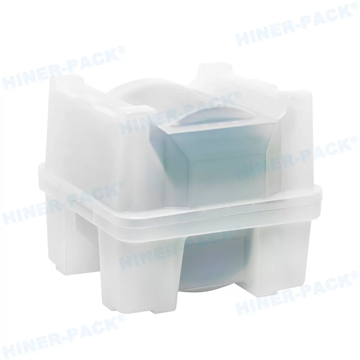
1. The 4 Engineering Benchmarks of a Tier-1 Wafer Boats Manufacturer
A precision semiconductor carrier must perform reliably under continuous mechanical, chemical, and thermal stress. When vetting a potential manufacturing partner, evaluate these four technical benchmarks:
Sub-Micron Tooling Tolerances: Automated robotic end-effectors require strict dimensional precision. Slot spacing, pocket depth, and robotic alignment notches must strictly comply with SEMI standards to prevent transfer errors and wafer edge chipping during high-speed pick-and-place cycles.
Permanent, Non-Migrating ESD Protection: Surface-treated antistatic sprays wash away during chemical baths and deionized (DI) water rinses. An advanced manufacturer must compound permanent conductive ($10^4 - 10^6\ \Omega/\text{sq}$) or static-dissipative ($10^6 - 10^9\ \Omega/\text{sq}$) polymer matrix networks compliant with ANSI/ESD S20.20.
Chemical Inertness & Trace Metal Purity: Carriers used in wet bench etching or cleaning must resist harsh acids (including HF and sulfuric acid) without leaching metallic ions or organic extractables into processing chemistries.
High-Temperature Dimensional Stability: For in-carrier baking, drying, or vacuum cure applications, materials must maintain high heat deflection temperatures (HDT) without pocket distortion or warpage.
2. Advanced Material Matrix for Semiconductor Wafer Boats
At Hiner-pack, our dedicated Polymer Material R&D Center—established in collaboration with university scientific research institutions—formulates specialized resins tailored to specific fab process environments:
| Polymer Formulation | Surface Resistivity (Ω/sq) | Max Continuous Temp | Chemical Compatibility | Primary Fab Process |
|---|---|---|---|---|
| Ultra-Clean Conductive PP | 10^4 - 10^6 (Permanent) | Up to 80°C | Standard Solvents & Mild Acids | Inter-bay AGV transfer, automated sorters, wafer shipping |
| Static-Dissipative Resin | 10^6 - 10^9 (Clean ESD) | 80°C - 120°C | DI Water, Dilute Acids | Cleanroom inspection bays, automated pick-and-place lines |
| High-Purity Modified PEEK / PES | 10^6 - 10^9 (or Insulative) | 150°C - 200°C+ | Superior Acid, Solvent & Steam Resistance | In-line wafer bake ovens, vacuum cure, harsh chemical baths |
| Fluoropolymer Blends (PFA / PTFE) | Custom Formulations | Up to 260°C | Exceptional (Hydrofluoric HF & Aggressive Etchants) | Wet bench etching, chemical stripping, diffusion transfer |
3. Turnkey Manufacturing Capabilities: Why Global Fabs Partner with Hiner-pack
Founded in 2013 in Shenzhen, China, Hiner-pack operates as an integrated high-tech enterprise. Sourcing directly from our precision facility provides distinct manufacturing advantages:
In-House Precision Tooling: Our mold engineering center utilizes high-speed CNC machining and mirror EDM systems to fabricate multi-cavity injection molds with strict tolerance control.
Cleanroom Injection Lines: Automated injection molding operates within controlled cleanroom environments, preventing airborne particulates from embedding in the molten polymer.
Proprietary Material Inventions & Patents: We hold numerous utility patents in conductive polymer formulations, enabling custom colored anti-static raw materials for clear fab lot identification.
Complete Carrier Integration: Consolidate your supply chain with our full product range, including Wafer Carrier Series (2" to 12"), Wafer Shipper Accessories (conductive sponges, cushions), JEDEC IC Trays, Waffle Packs, and Vacuum Release Gel Boxes.
4. Custom OEM/ODM Capabilities for Advanced Substrates
Beyond standard silicon wafers, compound semiconductors require specialized pocket geometries to prevent crystal micro-cracking:
Silicon Carbide (SiC) & Gallium Nitride (GaN): Customized edge-retention profiles and bevel clearances engineered specifically for dense, brittle wide-bandgap substrates.
Ultra-Thin Wafers (<100 μm): Low-friction slot entries and non-contact active area profiles prevent wafer bow and structural fracture during handling.
Fast DFM & Prototyping: Our engineering team provides complete Design for Manufacturability (DFM) reviews and 3D CAD models within 24 hours of receiving your specifications.
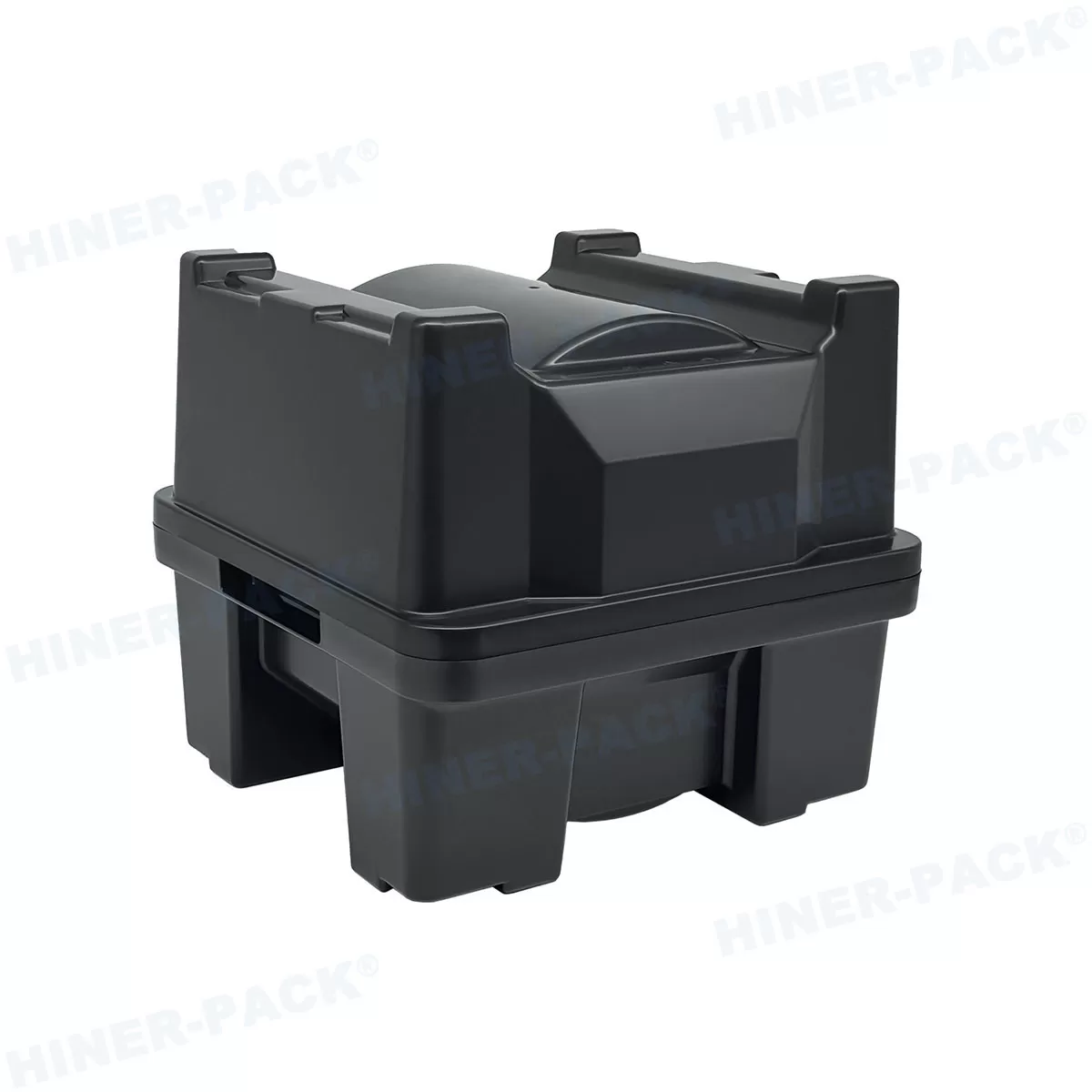
Engineering Verification & Sample Testing Program
Verify carrier compatibility with your cleanroom robotics and wet bench chemistry before volume procurement.
What Your Qualification Package Includes:
Free Evaluation Samples: 2 to 5 cleanroom-packaged wafer boats or cassettes dispatched within 48 hours for automated mechanical trials.
Full Engineering Documentation: 2D mechanical drawings, 3D .STEP CAD models, and official Certificates of Analysis (COA) for ESD and purity.
Direct Factory Pricing: Tiered volume quotations direct from our manufacturing plant, eliminating distributor and trading markups.
How to Request Your Kit:
Submit Your Parameters: Email your wafer diameter, substrate thickness, chemical/thermal exposure levels, and estimated batch volumes.
DFM & Tooling Review: Our engineering team verifies drawing clearances and confirms resin specifications within 24 hours.
Sample Testing: Receive evaluation samples via express courier within 48 hours for immediate fab qualification.
Fast-Track Engineering Desk: Contact our team directly at rainbowzhu@hiner-pack.com for immediate technical support.
Frequently Asked Questions About Choosing a Wafer Boats Manufacturer
Q1: What substrate sizes and carrier configurations does Hiner-pack produce as a wafer boats manufacturer?
A1: Hiner-pack designs and manufactures standard and custom wafer boats, cassettes, and storage carriers for 2-inch, 3-inch, 4-inch, 6-inch, 8-inch, and 12-inch wafers. Our portfolio includes 25-capacity multi-wafer cassettes, single-wafer shippers, coin-style boxes, and high-temperature matrix trays designed for silicon, SiC, GaN, and glass substrates.
Q2: How does Hiner-pack guarantee that wafer boats maintain dimensional stability in automated equipment?
A2: Through in-house CNC and EDM precision mold tooling, optical coordinate measuring machine (CMM) inspections, and optimized injection molding cycle parameters, we ensure that slot pitch, sidewall parallelism, and robotic pickup notches meet SEMI standards with minimal warpage across temperature cycles.
Q3: How does your factory ensure wafer carriers will not contaminate cleanroom environments?
A3: All carriers are molded from high-purity virgin resins, processed through multi-stage ultrasonic deionized water cleaning stations, and double-vacuum bagged inside an ISO-certified cleanroom environment. Every batch is certified for low particulate generation and zero volatile outgassing prior to shipment.
Q4: Why should semiconductor fabs partner directly with Hiner-pack rather than third-party distributors?
A4: Sourcing directly from Hiner-pack eliminates third-party markups (saving 15% to 30%), shortens custom tooling and prototype lead times, and provides direct engineering access to our polymer scientists and mold makers for custom substrate tailoring and complete batch traceability.
Ready to enhance your fab handling reliability? Contact our engineering desk at rainbowzhu@hiner-pack.com to discuss your project requirements with an established wafer boats manufacturer today.














