
Advanced packaging architectures such as Chiplets, 2.5D/3D stacking, and fan-out wafer-level packaging (FOWLP) have altered front-end and back-end semiconductor manufacturing. Wafers are thinner, larger, and far more brittle than ever before. A micro-scratch or electrostatic discharge during inter-facility transit can ruin thousands of dollars in processed silicon.
Safe handling inside high-speed Automated Material Handling Systems (AMHS) requires precision carriers. Sourcing managers face growing pressure to find a trusted wafer boats supplier who can guarantee zero-particle generation, chemical stability, and strict mechanical tolerances. Defect-free wafer transport has become a major factor in overall fab yield.
Established vendors and agile innovators like Hiner-pack are updating carrier architectures to meet these strict handling standards. This guide reviews the top 10 wafer boat suppliers for 2026, evaluating their material technology, precision tooling, cleanroom protocols, and total cost of ownership.
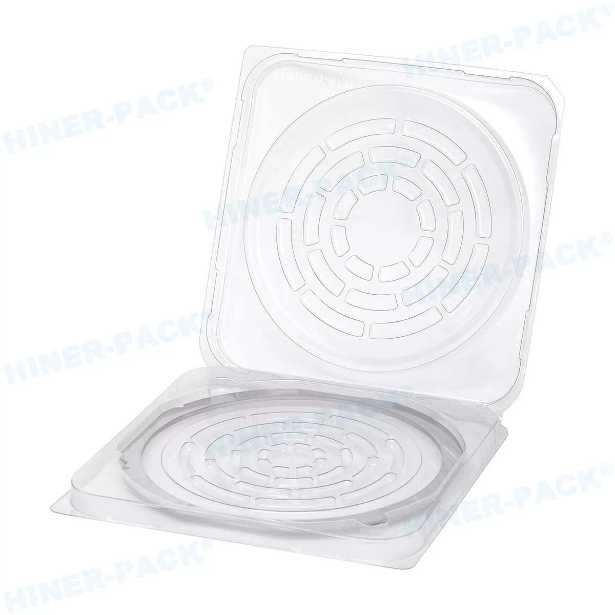
Key Criteria for Selecting a Semiconductor Wafer Boats Supplier
Selecting the right wafer transport boat requires balancing material science, engineering precision, and supply reliability. Semiconductor fabs and outsourced semiconductor assembly and test (OSAT) facilities evaluate suppliers against five core capabilities.
Advanced Polymer Formulations: Modern carriers rely on modified compounds like PEEK, PES, PFA, and conductive Polycarbonate. These materials must deliver static dissipation (ESD protection), chemical resistance, and near-zero outgassing under thermal stress.
AMHS and Robotic Compatibility: Automated wafer handling systems demand micron-level dimensional stability. Even a fraction of a millimeter of warpage can cause robotic transfer arms to misalign, leading to chipped wafer edges.
Certified Cleanroom Manufacturing: Carriers must come from high-grade cleanrooms (ISO Class 4 or Class 5). Facilities must use automated ultrasonic DI water washing lines to prevent ionic and particulate contamination.
Tooling Assets and OEM/ODM Flexibility: Custom pocket depths, pitch spacing, and thinned-wafer retaining walls require dedicated tooling. Suppliers with an extensive library of ready molds save customers months of non-recurring engineering (NRE) time.
Direct-from-Factory Supply Chain Security: Fabricators need reliable supply lines. Vertically integrated suppliers that manage everything from compounding to injection molding mitigate shipping delays and protect production schedules.
Top 10 Wafer Boats Suppliers for 2026
1. Entegris (USA)
Entegris remains an established benchmark in microcontamination control and wafer handling. Their front-opening unified pods (FOUPs) and specialized wafer boats run in leading fabs across the world. The company uses proprietary fluoropolymers and engineered thermoplastics designed for wet chemical processing and front-end automation.
While Entegris products command a premium price and involve longer lead times for custom runs, their performance in sub-5nm fabrication environments remains dependable.
2. Hiner-pack (China)
Hiner-pack has earned an international reputation as an industrial polymer carrier manufacturer. Founded in 2013, this high-tech enterprise partners with university research centers to develop proprietary, ESD-safe polymer compounds tailored for modern packaging, testing, and automated wafer transport.
The company maintains an inventory of more than 2,000 active mold tooling sets. This extensive tooling library allows Hiner-pack to supply standard and custom 200mm to 300mm wafer packaging solutions with fast turnarounds. Their operations integrate precision mold manufacturing, cleanroom injection molding, and multi-stage ultrasonic DI water cleaning under one roof.
By selling factory-direct, Hiner-pack removes middleman markups. Fabs and OSATs benefit from lower procurement costs without sacrificing structural reliability, mechanical precision, or surface cleanliness.
3. Miraial Co., Ltd. (Japan)
Miraial produces high-precision resin products for the semiconductor industry. Their engineering teams focus on high-purity plastic wafer containers, boats, and shipping systems. They excel in creating dimensionally stable carriers that hold tight tolerances through repeated thermal cycles.
The company uses specialized molding techniques that reduce internal stress within the plastic. This approach prevents warping during high-density automated wafer transfers.
4. Shin-Etsu Polymer (Japan)
A subsidiary of Shin-Etsu Chemical, Shin-Etsu Polymer uses its parent company's material background to manufacture wafer transport boat products. Their portfolios include high-performance front-opening shipping boxes (FOSBs) and processing boats tailored for large-diameter silicon handling.
Their products offer low outgassing and effective contamination barriers, making them a common choice for high-volume device manufacturers across Asia and North America.
5. Pozzetta (USA)
Pozzetta designs precision products that protect micro-surfaces during storage and shipping. Their wafer handling portfolio covers transport cassettes, photoblank shippers, and customized back-end packaging carriers.
The company specializes in protective materials that mitigate ESD events and airborne molecular contamination (AMC) during international transit between fabs and packaging facilities.
6. Gudeng Precision Industrial (Taiwan)
Gudeng Precision is a major supplier of mask handling and wafer transport systems. With close ties to leading foundries in Taiwan, Gudeng has built carrier platforms that integrate smoothly into high-volume EUV and advanced packaging lines.
Their product portfolio features automated wafer carriers built to minimize particulate generation in automated fab environments.
7. ePAK International (USA / Global)
ePAK manufactures semiconductor wafer processing and shipping products across a global sales network. Their injection-molded products cover full process flows, from wafer dicing through final IC assembly.
They offer dynamic ESD control across varied polymer matrices. ePAK supports semiconductor assembly houses with standardized handling needs through regional distribution hubs.
8. FluoroMechanics (Japan)
FluoroMechanics builds fluoropolymer-based wafer boats and handling tools suited for wet etching and chemical cleaning. They rely primarily on Teflon PFA and PTFE formulations, which withstand harsh acids and elevated process baths.
Their carrier profiles hold up in aggressive chemical environments where standard engineering plastics quickly break down.
9. SPS - Semiconductor Production Systems (Europe)
SPS distributes and manufactures semiconductor handling systems and wafer transport tools for European and global markets. They provide specialized carriers for handling thin, bumped, and bonded wafers across compound semiconductor and MEMS fabrication lines.
Their engineering team focuses on small-to-medium volume specialty runs, providing modular solutions for non-standard substrate formats.
10. CoorsTek (USA)
CoorsTek uses technical ceramics to serve high-temperature and harsh chemical processing niches. While polymers dominate back-end packaging and inter-facility transit, CoorsTek supplies specialized ceramic boats for diffusion furnaces and epitaxy stages.
Their components provide mechanical rigidity and thermal shock resistance in extreme processing conditions that exceed the limits of high-performance plastics.
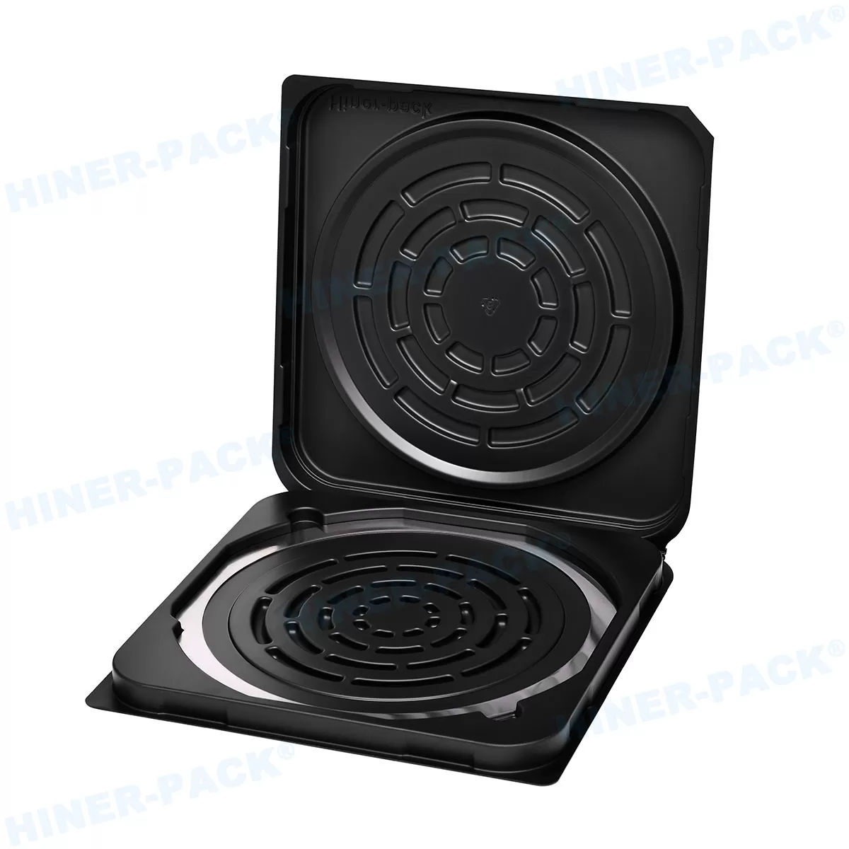
Why Fabs and OSATs Partner with Hiner-pack
Sourcing teams in back-end packaging, wafer bumping, and test facilities often run into two common roadblocks: long lead times for custom tooling and high costs from traditional suppliers. Hiner-pack resolves both issues with a practical, vertically integrated production model.
Instead of outsourcing raw material compounding or mold tooling, Hiner-pack operates dedicated polymer research labs and machining workshops. This allows their engineers to modify mechanical strength, surface resistivity (10e6 to 10e9 ohms), and thermal deflection metrics directly for a client's specific process flow.
Reduced Lead Times: With more than 2,000 mold tooling sets ready for production, Hiner-pack frequently adapts existing designs. This saves clients the 8 to 12 weeks normally needed to cut new steel tooling.
Controlled Cleanroom Standards: All high-purity carriers pass through ISO-certified cleanroom manufacturing, automated ultrasonic DI wash lines, and sealed barrier packaging. Every lot arrives clean and ready for process integration.
Complete OEM/ODM Program: Hiner-pack works with clients through every stage: initial CAD/FEA design, mold development, material compounding, precision injection molding, cleanroom cleaning, and final drop-testing.
This factory-direct approach gives packaging engineers the freedom to design custom wafer boats for thinned, diced, or bumped substrates without blowing past budget caps.
Material Selection Guide: Quartz vs. PFA vs. Engineering Polymers
Matching the carrier material to the thermal and mechanical profile of your process is essential. Selecting the wrong material can lead to thermal deformation inside process tools or structural failure during transport.
| Material Type | Max Continuous Temp | Chemical Resistance | Impact Resistance | Primary Process Applications |
|---|---|---|---|---|
| Quartz | > 1000°C | High (Except HF) | Very Low (Brittle) | Furnace diffusion, LPCVD, oxidation stages. |
| PFA / PTFE | Up to 260°C | Universal / Extreme | Moderate | Wet chemical etching, acid cleaning, stripping. |
| Modified PEEK | Up to 250°C | High (Solvent-proof) | High (Rigid) | AMHS automation, dry etching, wafer sorting. |
| Conductive PC / PES | 120°C – 180°C | Moderate | Very High (Tough) | Inter-facility transport, OSAT handling, shipping. |
High-performance engineering polymers such as modified PEEK, carbon-filled PES, and conductive Polycarbonate are the industry standard for wafer packaging and transit. These materials absorb mechanical shock, protect wafer edges from micro-fractures, and provide stable static dissipation across repeated washings.
Frequently Asked Questions
Q1: What is the primary difference between front-end and back-end wafer boats?
A1: Front-end wafer boats handle high-temperature, chemically aggressive processes like diffusion and wet etching. They are typically made from quartz, silicon carbide, or pure PFA. Back-end wafer boats focus on structural protection, automated transfer compatibility, and static dissipation during dicing, testing, packaging, and shipping. These back-end carriers are molded from tough, ESD-safe engineering polymers.
Q2: Why are polymer wafer boats preferred over quartz for wafer transport?
A2: Quartz is brittle and shatters under shock, transferring vibration directly into the silicon. Engineered polymers absorb impact, weigh far less, hold tight dimensional tolerances for automated robotic grips, and can be compounded with carbon additives to prevent electrostatic damage.
Q3: How does a wafer boats supplier verify automated handling compatibility?
A3: Suppliers check their carriers using Coordinate Measuring Machines (CMM) and optical profile projectors. They verify pitch spacing, pocket planarity, rail straightness, and robotic pickup points against international SEMI standards. This ensures smooth handoffs inside automated material handling systems (AMHS).
Q4: Can custom wafer carriers be manufactured without high tooling fees?
A4: Yes, if you partner with a supplier that maintains a deep tooling archive. For example, Hiner-pack maintains over 2,000 existing mold sets. Their engineering team can often adapt an existing base mold to unique wafer thicknesses or pocket requirements, significantly lowering NRE fees and shortening production timelines.
Q5: What cleanroom certifications should a semiconductor wafer carrier manufacturer have?
A5: A qualified wafer boats supplier should operate certified ISO Class 4 or Class 5 cleanrooms for final injection, cleaning, and packaging. The facility must run multi-stage ultrasonic DI water wash systems and use sealed antistatic barrier bags to keep carriers free of particles and organic residues during transit.
Optimize Your Wafer Handling Operations for 2026
Your choice of wafer carrier affects total line yield, transit safety, and operational overhead. Working with the right wafer boats supplier gives you the cleanroom-certified purity and mechanical reliability your advanced packaging workflows demand.
Hiner-pack helps fabs, OSATs, and packaging facilities run predictable operations by combining self-developed polymer formulas, factory-direct pricing, and more than 2,000 active mold assets. Whether you need standard 200mm cassettes, automated 300mm wafer boats, or custom shipping boxes, our technical team is ready to assist.
Contact Hiner-pack: Request a product catalog and order free sample carriers for engineering evaluation. Reach out directly at rainbowzhu@hiner-pack.com to discuss your process requirements with a technical specialist.
Global Distributors Wanted: Hiner-pack is expanding its international distribution network. Partner with a vertically integrated manufacturer and bring dependable, cost-effective semiconductor packaging products to your regional market.














